4.1. MOSFET Devices
4.1.1. nmos
Device Information
Property |
Value |
|---|---|
Description |
n-channel enhancement MOS transistor - Low Voltage (LV) |
Device Recognition |
Activ, GatPoly |
Model Name |
sg13_lv_nmos |
Layout Cell Name |
sg13g2_pr - nmos |
Parameters |
w, l, ng, m |
Netlist Syntax |
MN1 D G S B sg13_lv_nmos w=150.00n l=130.00n m=1 ng=1 |
Additional Notes |
Can be placed in nWell-hole/nBuLay box for isolated nmosi device. |
Parameters Information
Parameter |
Description |
Schematic-View |
LVS-View |
LVS-Comparison |
|---|---|---|---|---|
w |
Transistor width |
✅ |
✅ |
✅ |
l |
Transistor channel length |
✅ |
✅ |
✅ |
m |
Number of transistors (multiplicity) |
✅ |
❌ |
❌ |
ng |
Number of gates |
✅ |
❌ |
❌ |
Tip
The m parameter is implicitly calculated in the layout extracted netlist within the value of the w parameter, which represents the total width.
Example: MN0 D G S B sg13_lv_nmos w=1u l=1u m=2, this will be recognized as MN0 D G S B sg13_lv_nmos w=2u l=1u
See Figure 4.1.1 for an explanation.
The ng parameter will be ignored, as the w represents total width of all fingers.
The finger width (WF) is defined as w/ng
Example: MN0 D G S B sg13_lv_nmos w=1u l=1u ng=2, this will be recognized as MN0 D G S B sg13_lv_nmos w=1u l=1u
See Figure 4.1.1 for an explanation.
Layout Information (Refer to Layout Layers)
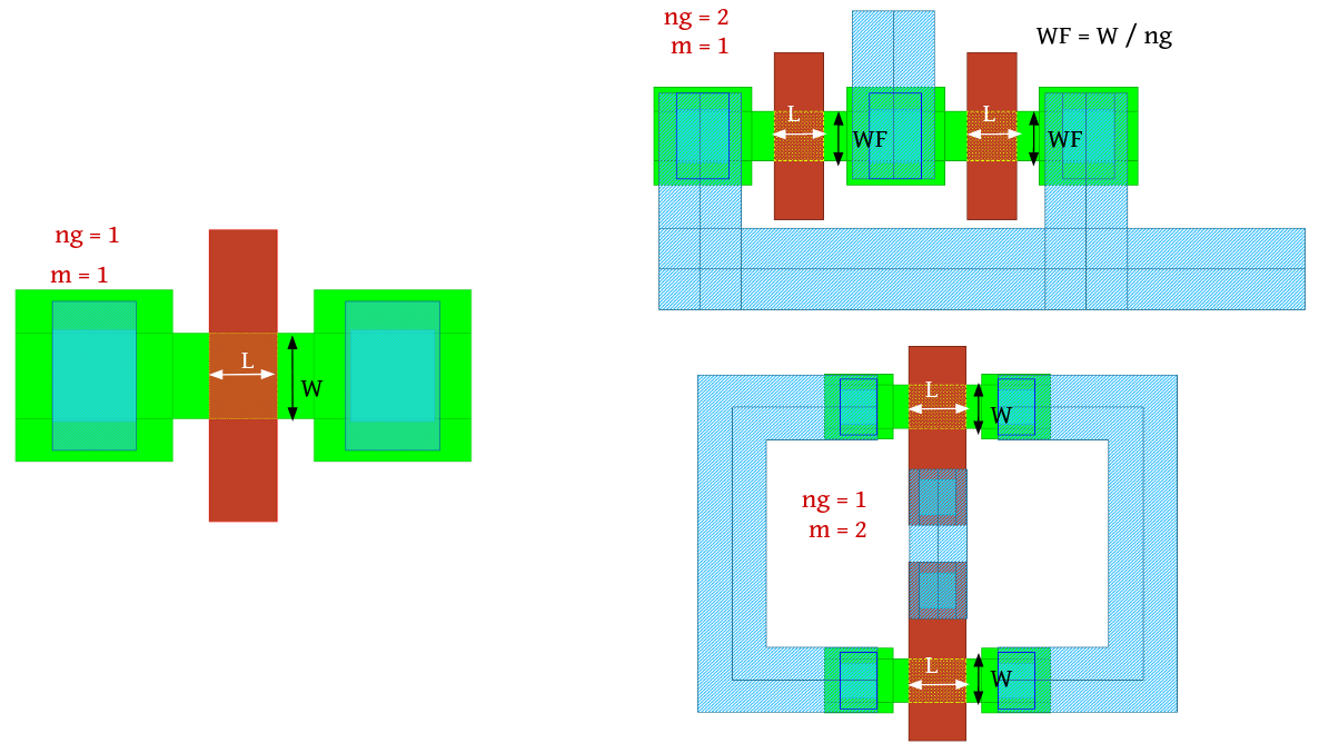
Figure 4.1.1 Layout for nMOS-LV transistor
4.1.2. nmosHV
Device Information
Property |
Value |
|---|---|
Description |
n-channel enhancement MOS transistor with max SD voltage of 3.3V - High Voltage (HV) |
Device Recognition |
Activ, GatPoly, ThickGateOx |
Model Name |
sg13_hv_nmos |
Layout Cell Name |
sg13g2_pr - nmosHV |
Parameters |
w, l, ng, m |
Netlist Syntax |
MN1 D G S B sg13_hv_nmos w=0.6u l=0.45u ng=1 m=1 |
Additional Notes |
Can be placed in nWell-hole/nBuLay box for isolated nmosi device. |
Parameters Information
Parameter |
Description |
Schematic-View |
LVS-View |
LVS-Comparison |
|---|---|---|---|---|
w |
Transistor width |
✅ |
✅ |
✅ |
l |
Transistor channel length |
✅ |
✅ |
✅ |
m |
Number of transistors (multiplicity) |
✅ |
❌ |
❌ |
ng |
Number of gates |
✅ |
❌ |
❌ |
Tip
The m parameter is implicitly calculated in the layout extracted netlist within the value of the w parameter, which represents the total width.
Example: MN0 D G S B sg13_hv_nmos w=1u l=1u m=2, this will be recognized as MN0 D G S B sg13_hv_nmos w=2u l=1u
See Figure 4.1.1 for an explanation.
The ng parameter will be ignored, as the w represents total width of all fingers.
The finger width (WF) is defined as w/ng
Example: MN0 D G S B sg13_hv_nmos w=1u l=1u ng=2, this will be recognized as MN0 D G S B sg13_hv_nmos w=1u l=1u
See Figure 4.1.1 for an explanation.
Layout Information (Refer to Layout Layers)
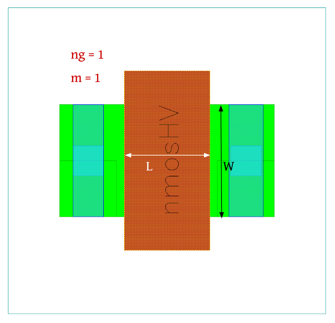
Figure 4.1.2 Layout for nMOS-HV transistor
4.1.3. pmos
Device Information
Property |
Value |
|---|---|
Description |
p-channel enhancement MOS transistor - Low Voltage (LV) |
Device Recognition |
Activ, GatPoly, pSD, Nwell |
Model Name |
sg13_lv_pmos |
Layout Cell Name |
sg13g2_pr - pmos |
Parameters |
w, l, ng, m |
Netlist Syntax |
MP1 D G S B sg13_lv_pmos w=150.00n l=130.00n ng=1 m=1 |
Parameters Information
Parameter |
Description |
Schematic-View |
LVS-View |
LVS-Comparison |
|---|---|---|---|---|
w |
Transistor width |
✅ |
✅ |
✅ |
l |
Transistor channel length |
✅ |
✅ |
✅ |
m |
Number of transistors (multiplicity) |
✅ |
❌ |
❌ |
ng |
Number of gates |
✅ |
❌ |
❌ |
Tip
The m parameter is implicitly calculated in the layout extracted netlist within the value of the w parameter, which represents the total width.
Example: MP0 D G S B sg13_lv_pmos w=1u l=1u m=2, this will be recognized as MP0 D G S B sg13_lv_pmos w=2u l=1u
See Figure 4.1.2 for an explanation.
The ng parameter will be ignored, as the w represents total width of all fingers.
The finger width (WF) is defined as w/ng
Example: MP0 D G S B sg13_lv_pmos w=1u l=1u ng=2, this will be recognized as MP0 D G S B sg13_lv_pmos w=1u l=1u
See Figure 4.1.2 for an explanation.
Layout Information (Refer to Layout Layers)

Figure 4.1.3 Layout for pMOS-LV transistor
4.1.4. pmosHV
Device Information
Property |
Value |
|---|---|
Description |
p-channel enhancement MOS transistor with max SD voltage of 3.3V - High Voltage (HV) |
Device Recognition |
Activ, GatPoly, pSD, Nwell, ThickGateOx |
Model Name |
sg13_hv_pmos |
Layout Cell Name |
sg13g2_pr - pmosHV |
Parameters |
w, l, ng, m |
Netlist Syntax |
MP1 D G S B sg13_hv_pmos w=0.3u l=0.4u ng=1 m=1 |
Parameters Information
Parameter |
Description |
Schematic-View |
LVS-View |
LVS-Comparison |
|---|---|---|---|---|
w |
Transistor width |
✅ |
✅ |
✅ |
l |
Transistor channel length |
✅ |
✅ |
✅ |
m |
Number of transistors (multiplicity) |
✅ |
❌ |
❌ |
ng |
Number of gates |
✅ |
❌ |
❌ |
Tip
The m parameter is implicitly calculated in the layout extracted netlist within the value of the w parameter, which represents the total width.
Example: MP0 D G S B sg13_hv_pmos w=1u l=1u m=2, this will be recognized as MP0 D G S B sg13_hv_pmos w=2u l=1u
See Figure 4.1.1 for an explanation.
The ng parameter will be ignored, as the w represents total width of all fingers.
The finger width (WF) is defined as w/ng
Example: MP0 D G S B sg13_hv_pmos w=1u l=1u ng=2, this will be recognized as MP0 D G S B sg13_hv_pmos w=1u l=1u
See Figure 4.1.1 for an explanation.
Layout Information (Refer to Layout Layers)
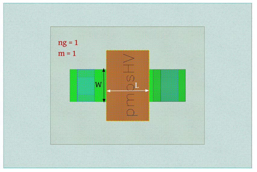
Figure 4.1.4 Layout for pMOS-HV transistor