4.3. BJT Devices
4.3.1. npn13G2
Device Information
Property |
Value |
|---|---|
Description |
npn SiGe:C HBT high performance device, 300 GHz fT. Layout configuration BEC |
Device Recognition |
Activ, nSD.blk, TRANS, EmWind, ptab (pSD + Activ.mask) |
Model Name |
npn13G2 |
Layout Cell Name |
sg13g2_pr - npn13G2 |
Parameters |
We, le, AE, PE, m/NE |
Netlist Syntax |
Q1 C B E sub! npn13G2 le=900.0n we=70.00n m=1 |
Parameters Information
Parameter |
Description |
Schematic-View |
LVS-View |
LVS-Comparison |
|---|---|---|---|---|
we |
Emitter width (Fixed) |
❌ |
❌ |
❌ |
le |
Emitter length (Fixed) |
❌ |
❌ |
❌ |
AE |
Emitter area (Fixed), will be calculated from WE/LE if not explicitly provided. |
❌ |
✅ |
✅ |
PE |
Emitter perimeter (Fixed), will be calculated from WE/LE if not explicitly provided. |
❌ |
✅ |
✅ |
m/NE |
Number of BJTs/Emitters (multiplicity) |
❌ |
✅ |
✅ |
Tip
The npn13G2 device has fixed dimensions, (WE = 0.07u & LE = 0.9u).
You have the option to use either WE/LE or AE/PE in your netlist.
Layout Information (Refer to Layout Layers)
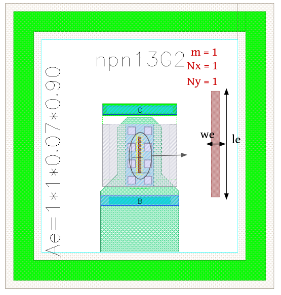
Figure 4.3.1 Layout for NPN13G2 bipolar transistor
4.3.2. npn13G2L
Device Information
Property |
Value |
|---|---|
Description |
npn SiGe:C scalable HBT high performance device, 280 GHz fT. Layout configuration BEC |
Device Recognition |
Activ, TRANS, EmWind, ptab (pSD + Activ.mask) |
Model Name |
npn13G2l |
Layout Cell Name |
sg13g2_pr - npn13G2L |
Parameters |
We, le, AE, PE, m/NE |
Netlist Syntax |
Q1 net1 net2 net3 sub! npn13G2l le=1.0u we=70.00n m=1 |
Parameters Information
Parameter |
Description |
Schematic-View |
LVS-View |
LVS-Comparison |
|---|---|---|---|---|
we |
Emitter width (Fixed) |
❌ |
❌ |
❌ |
le |
Emitter length |
❌ |
❌ |
❌ |
AE |
Emitter area, will be calculated from WE/LE if not explicitly provided. |
❌ |
✅ |
✅ |
PE |
Emitter perimeter, will be calculated from WE/LE if not explicitly provided. |
❌ |
✅ |
✅ |
m/NE |
Number of BJTs/Emitters (multiplicity) |
❌ |
✅ |
✅ |
Tip
The npn13G2L device has fixed width (WE = 0.07u), its length (LE) could vary from [1:2.5]u.
You have the option to use either WE/LE or AE/PE in your netlist.
Layout Information (Refer to Layout Layers)
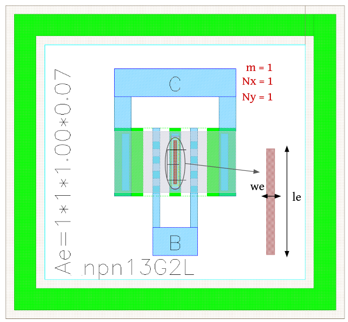
Figure 4.3.2 Layout for NPN13G2L bipolar transistor
4.3.3. npn13G2V
Property |
Value |
|---|---|
Description |
npn SiGe:C scalable HBT high voltage device, 90 GHz fT. Layout configuration BEC |
Device Recognition |
Activ, TRANS, EmWiHV, ptab (pSD + Activ.mask) |
Model Name |
npn13G2v |
Layout Cell Name |
sg13g2_pr - npn13G2V |
Parameters |
We, le, AE, PE, m/NE |
Netlist Syntax |
Q1 net1 net2 net3 sub! npn13G2v le=1.0u we=120.00n m=1 |
Parameters Information
Parameter |
Description |
Schematic-View |
LVS-View |
LVS-Comparison |
|---|---|---|---|---|
we |
Emitter width (Fixed) |
❌ |
❌ |
❌ |
le |
Emitter length |
❌ |
❌ |
❌ |
AE |
Emitter area, will be calculated from WE/LE if not explicitly provided. |
❌ |
✅ |
✅ |
PE |
Emitter perimeter, will be calculated from WE/LE if not explicitly provided. |
❌ |
✅ |
✅ |
m/NE |
Number of BJTs/Emitters (multiplicity) |
❌ |
✅ |
✅ |
Tip
The npn13G2V device has fixed width (WE = 0.12u), its length (LE) could vary from [1:5.0]u.
You have the option to use either WE/LE or AE/PE in your netlist.
Layout Information (Refer to Layout Layers)
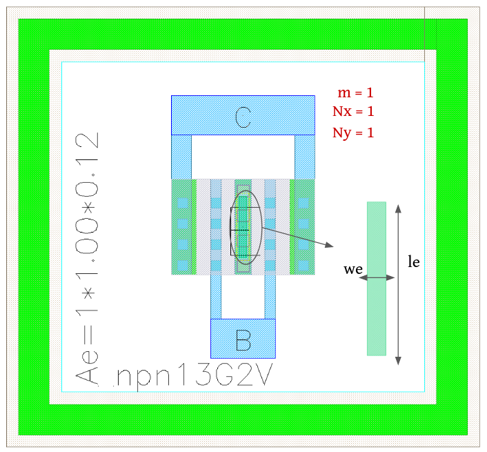
Figure 4.3.3 Layout for NPN13G2V bipolar transistor
4.3.4. pnpMPA
Device Information
Property |
Value |
|---|---|
Description |
HBT pnp used for BandGap Reference (BGR) circuit |
Device Recognition |
Activ, NWell, nBuLay, pSD |
Model Name |
pnpMPA |
Layout Cell Name |
sg13g2_pr - pnpMPA |
Parameters |
l, w, a, p, m/NE |
Netlist Syntax |
Q1 sub! net1 net2 pnpMPA a=1.4p p=5.4u m=1 |
Parameters Information
Parameter |
Description |
Schematic-View |
LVS-View |
LVS-Comparison |
|---|---|---|---|---|
W |
Emitter width |
✅ |
✅ |
❌ |
L |
Emitter length |
✅ |
✅ |
❌ |
A |
Emitter area, will be calculated from W/L if not explicitly provided. |
❌ |
✅ |
✅ |
P |
Emitter perimeter, will be calculated from W/L if not explicitly provided. |
❌ |
✅ |
✅ |
m/NE |
Number of BJTs/Emitters (multiplicity) |
❌ |
✅ |
✅ |
Tip
You have the option to use either W/L or A/P in your netlist.
In KLayout netlist browser’s display mode, the A/P parameters will be mapped to AE/PE.
Layout Information (Refer to Layout Layers)
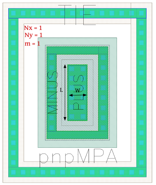
Figure 4.3.4 Layout for pnpMPA bipolar transistor