Introduction
This document gives an overview of the open source EM ecosystem with simulation tools and workflows and utilities for IHP SG13G2 OPDK.
This document was updated on February 04, 2026.
Solver methods
Two different solver methods are supported now:
FDTD (finite difference in time domain) using the openEMS solver workflow
FEM (finite elements in frequency domain) using the AWS Palace solver workflow.
Both methods use full 3D volume meshing, but have their specific strengths and weaknesses, so the choice of the most efficient solver also depends of the device under test. This will be discussed later in this document.
One additional FEM solver solution, ElmerFEM by CSC, is implemented in the workflow as an early technology preview, but needs additional development regarding solver features.
At the present time, there is no Method of Moments open source solver available which fits the needs of our RFIC EM workflow (lossy thick metals in layer lossy dielectrics). Known open source MoM solvers are designed for radar scattering problems in free space, or wire antenna simulation. An open source equivalent for Sonnet or ADS Momentum could not be found at the present time, so all EM modeling must be done using FEM or FDTD.
Which solver method is better for my model?
Here are some aspects that might help to choose a solver method:
FDTD uses a pulse excitation and always gives wide band sweep results using FFT. This means that we can get detailed, wide band data with no extra effort, whereas FEM requires each frequency point to be simulated one after another.
If we have multiple ports, FDTD requires to run a separate excitation for each port to get the full S-matrix, so that full n-port simulation will take approximately n times longer than a single port excitation. Only if we can apply symmetry or don’t need all possible signal paths, we can simulate a reduced number of port excitations. This is different in Palace FEM, where multi-port models also requires more simulation time than a single port, but scale nicer than linear.
FDTD requires much less memory for simulation, you can simulate most RFIC models easily on a machine with 16 GB RAM. For FEM, models can become much larger, and 16 GB is only sufficient for small models with limited mesh density. If your computer’s RAM is limited, FDTD will enable simulation where FEM already runs out of memory.
If you have a large model with many cells, e.g. antenna model that is many wavelength in each direction, FDTD is nice because memory scales linear O(N) with problem size: if we double the number of mesh cells, it only takes 2x the memory and 2x the simulation time (assuming the same time step, i.e. same minimum mesh cell size). In comparison, FEM simulation will require more RAM and that RAM requirement will scale more than linear O(N1,5) when increasing the model size.
FDTD uses a rectangular Cartesian mesh where each mesh line divides the entire simulation domain. There is no local mesh refinement, so any small mesh resolution will propagate across the entire simulation domain, as shown in the screenshot below.
This is often a disadvantage, but on the positive side, we can use this if our layout has much dummy metal fill: once we have mesh lines for metal on one layer, extra metal stacked on other layers in that area will not increase model complexity, it doesn’t matter if the material modeled there is oxide or metal.
FDTD becomes inefficient if we need to resolve very small geometry detail, which results in small mesh cell, which results in a small time step. This will then increase the total number of time steps required for simulation. In the IHP openEMS workflow, the smallest mesh size is limited by parameter refined_cellsize, but also by thickness of metal layers. Often, the overall value is set by Metal1 layer thickness at 0.42 µm. This is modeled with 1 mesh cell thickness. Besides resolving geometry detail and gaps, there are more aspects for refined_cellsize, for example to model skin effect in the conductor volumes: skin depth is 0.8µm at 10 GHz and 0.25µm at 100 GHz.
- One important aspect in choosing the solver method is meshing at diagonal lines: in FDTD, the xyz-oriented mesh will create staircase artifacts along the diagonals, and might even create short circuit between turns if simulation parameter refined_cellsize is too large. On the other hand, using a small value for refined_cellsize will lead to many mesh cells and possibly small time step, which slows down simulation.FEM is a clear winner here, because it can use variable mesh orientation and local mesh refinement, for efficient simulation of diagonal and curved shapes as well as local mesh refinement for small detail.
FDTD is a clear winner for electrically large models (many wavelength in each direction) if the smallest mesh size (→ timestep) is reasonable. One example is antennas: simulation volume is typically many wavelengths cubed, and only one excitation must be simulated, for single port or simultaneous excitation of multiple ports in an array.
One strength of the AWS Palace FEM workflow is that we can switch to a „quick & dirty“ simulation using 1st order FEM basis functions, which is less accurate but much faster than the regular setting (2nd order FEM basis function). This is nice to do a pre-check of the simulation, to see if we made mistakes with ports or metal routing. With openEMS FDTD, if refined_cellsize is already limited by staircasing and possible shorts between metal traces, we have no other switch to do a fast simulation with reduced accuracy. We could only reduce the energy convergence limit where simulation is considered finished, but that usually saves not much time and comes with much higher ripple in simulation results.
In summary, for circuit level models (no antennas), FEM using AWS Palace is often the faster simulator. It requires more RAM than openEMS FDTD, but on a machine with 64 GB or more a wide range of models can be simulated. If only 16 GB is available, openEMS is the better choice to avoid running out of memory.
For antennas, openEMS is a proven solution, whereas Palace antenna pattern calculation is rather new and needs more evaluation.
Workflows using Python model script
For both solver methods, openEMS FDTD and Palace FEM, a script-based workflow (Python) is available where the user defines one GDSII layout file to be simulated, plus a pre-configured XML stackup file, plus a few simulation settings. The workflow then creates the 3D simulation model and simulates it, providing an S-parameter output file.
New: the workflows can also be installed as a Python module (pip install), so that a local copy of the workflow module is no longer required in the simulation directory.
gds2openEMS workflow (FDTD)
Installation as a Python module using Pypi, instead of local modules folder in model directory:
pip install gds2openEMS
More info on installing as a module: https://pypi.org/project/gds2openEMS/
gds2palace workflow (FEM)
Installation as a Python module using Pypi:
More info on installing as a module: https://pypi.org/project/gds2palace/
Important: Both workflows use an XML stackup file, but there are some differences in the details. For example, the MIM capacitor layer is modeled differently to achieve best simulation performance for each solver method: avoid small dimension for FDTD, use thick equivalent layer with high permittivity instead, resulting in same capacitance. For each solver, use the stackups from the respective workflow repository.
Graphical user interface: EMStudio
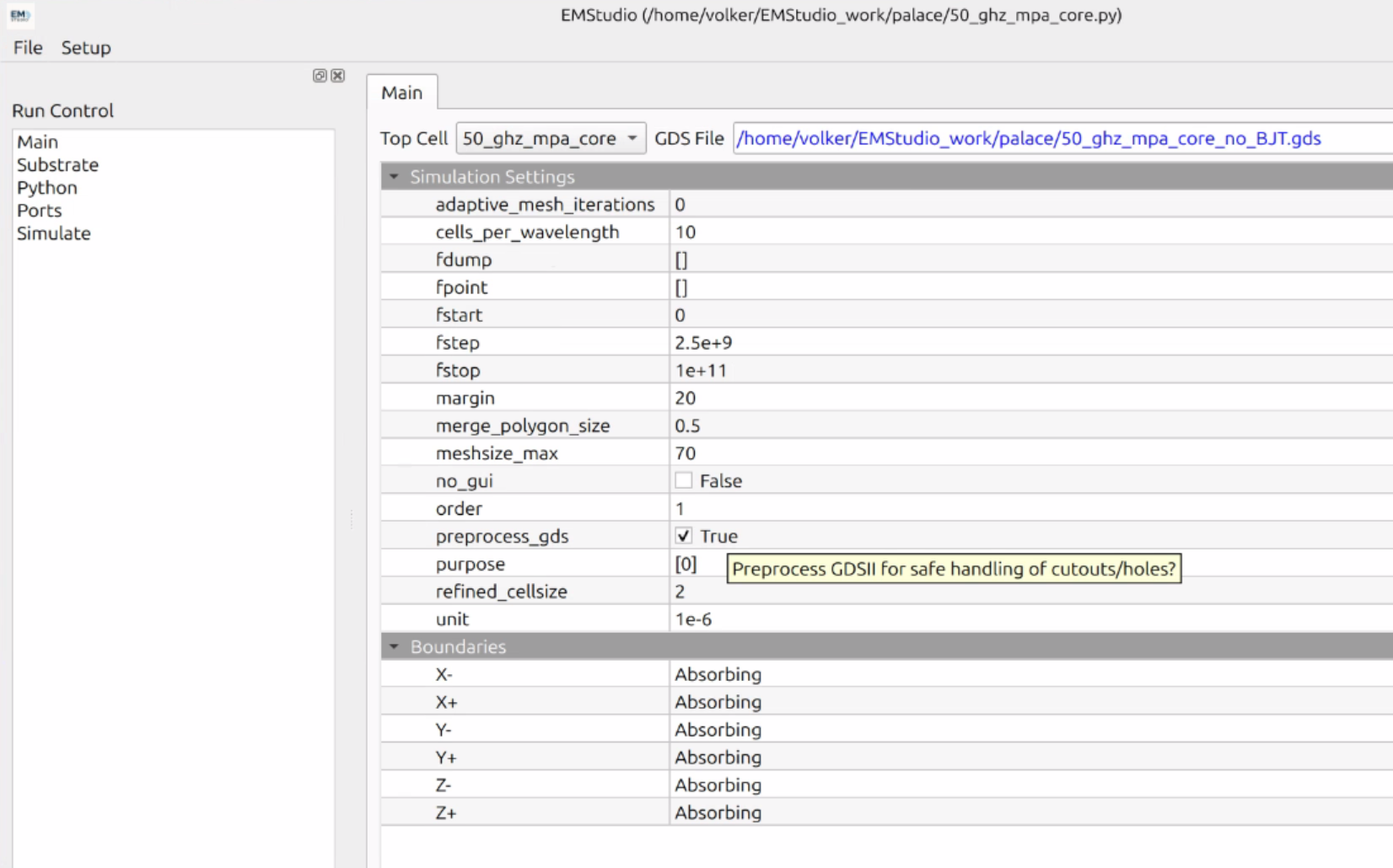
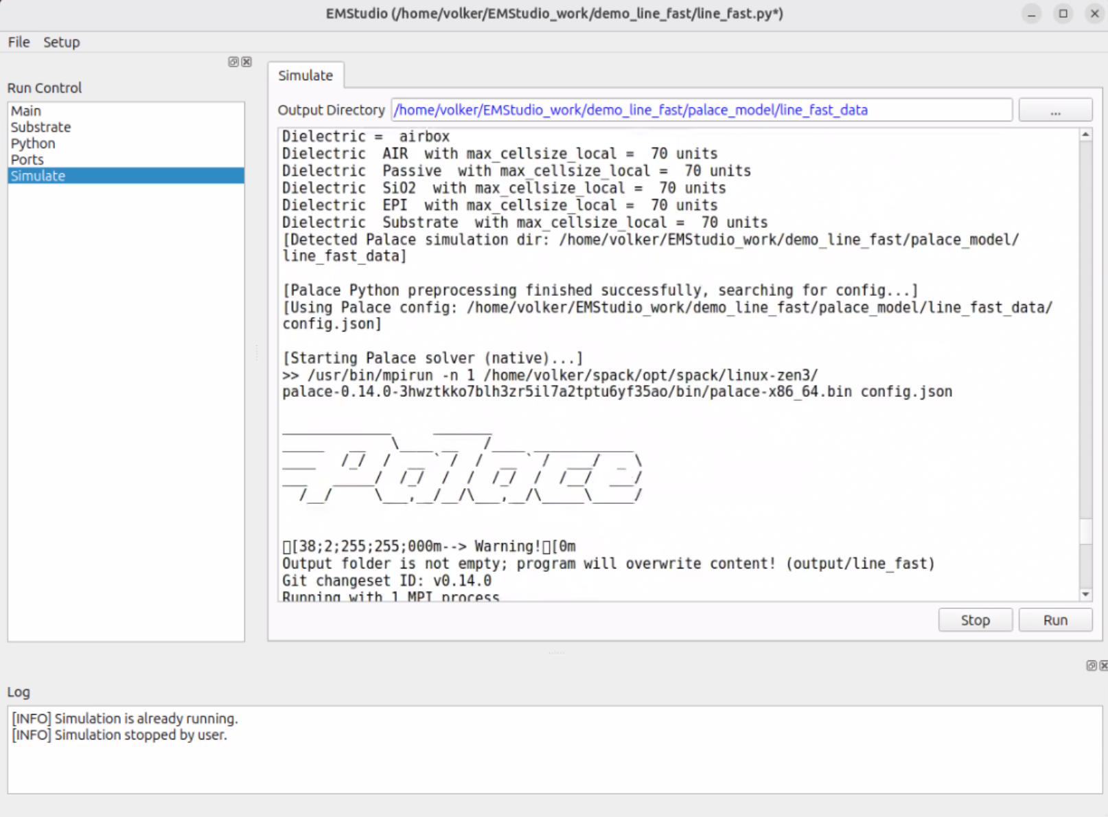
A graphical user interface is provided by IHP that support both openEMS and Palace workflows, with bi-directional sync between user interface settings and a built-in script editor. Note that this is a user interface only, and requires all the regular workflow components to be already installed. EMStudio will then call the workflows and also start the solver.
https://github.com/IHP-GmbH/EMStudio
EMStudio is available for Windows and Linux. For Linux, follow instructions to build the software from the github repository. For Windows, a setup file is provided, see instructions in github readme.
Graphical user interface: setupEM
setupEM is a graphical user interface for the gds2palace FEM workflow, which is co-developed with that workflow, to offer the most relevant features in an intuitive package, built from one single Python file.
Different from EMStudio, setupEM is always controlled from the GUI and the resulting script can be displayed, but there is no built-in script editor and no bi-directional sync from Code to GUI and vice versa. Existing scripts can be imported to get their settings, but the structure of the resulting model file is hard coded and extra code sections from an imported file will be ignored.
setupEM covers typical use cases with one single GDSII file, where each port is excited for full S-parameter data. Antenna far field pattern and multi-chip configuration with mixed technologies are not supported yet.
Installation as a Python module using Pypi:
Installing the setupEM Python module will also install gds2palace and all dependencies, so you don’t need to install that manually.
S-Parameter port de-embedding
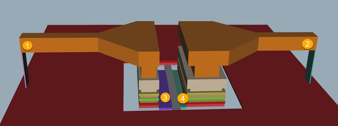
The IHP workflows for openEMS and Palace use lumped ports for simulation, which have a physical size between the signal and ground terminal. The size of these ports is included in simulation results and shows up as extra length (phase, inductance).
If the device under test itself is really small, like the T-junction in the screenshot below, the relative error from these port parasitics can be significant.
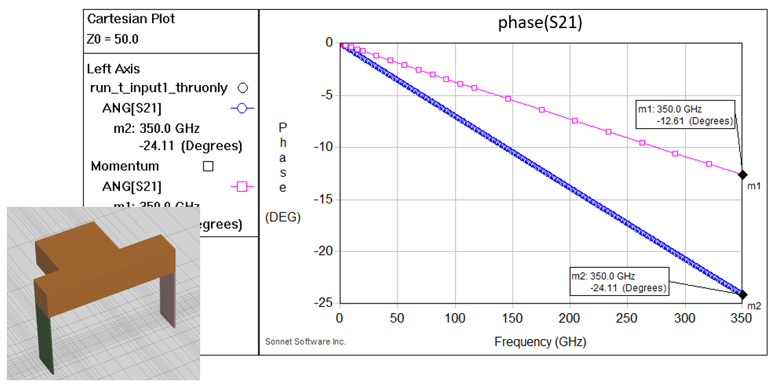
Different methods have been tested to remove this port discontinuity in postprocessing. The problem can be solved rigorously using calibration techniques known from network analyzer calibration, but that would require a lot of overhead for EM simulation of calibration standards.
The most practical solution is to estimate the inductance of the lumped port, and subtract that series inductance from EM simulation results.
Port de-embedding in Palace workflow
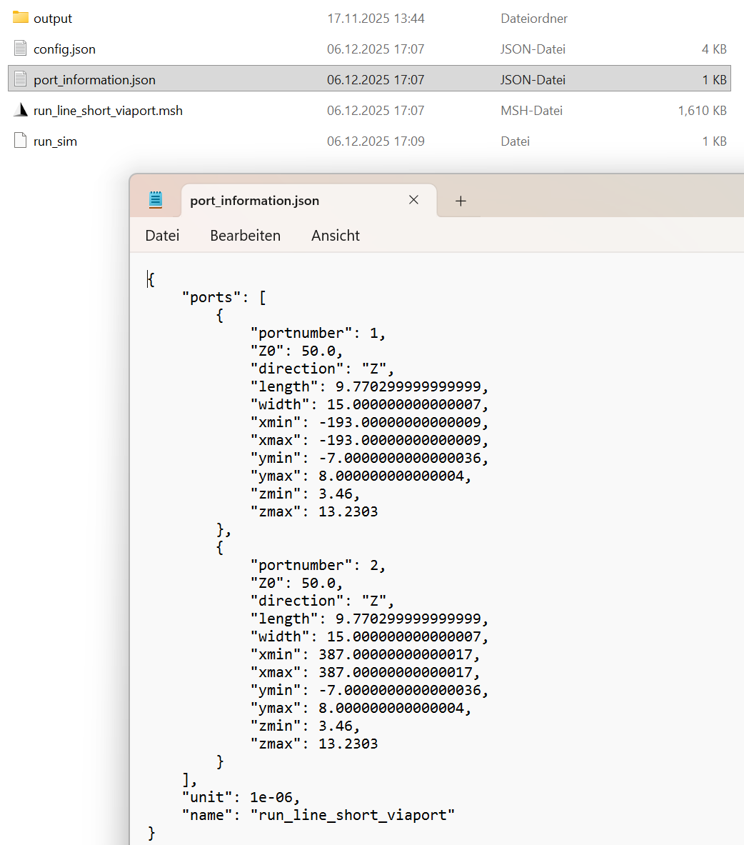
This solution was implemented in the S-parameter postprocessing script for the gds2palace flow: first, simulation results are converted from Palace *.csv files to Touchstone *.snp, and then inductance of the ports is estimated using port geometry information that was written by gds2palace to the port_information.json metadata file.
gsd2palace postprocessing script combine_snp runs Python file combine_extend_snp.py which does the actual de-embedding. These scripts can be found at:
https://github.com/VolkerMuehlhaus/gds2palace_ihp_sg13g2/tree/main/scripts
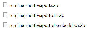
The de-embedded data is then written into a separate file with suffix „deembedded“, as shown below:
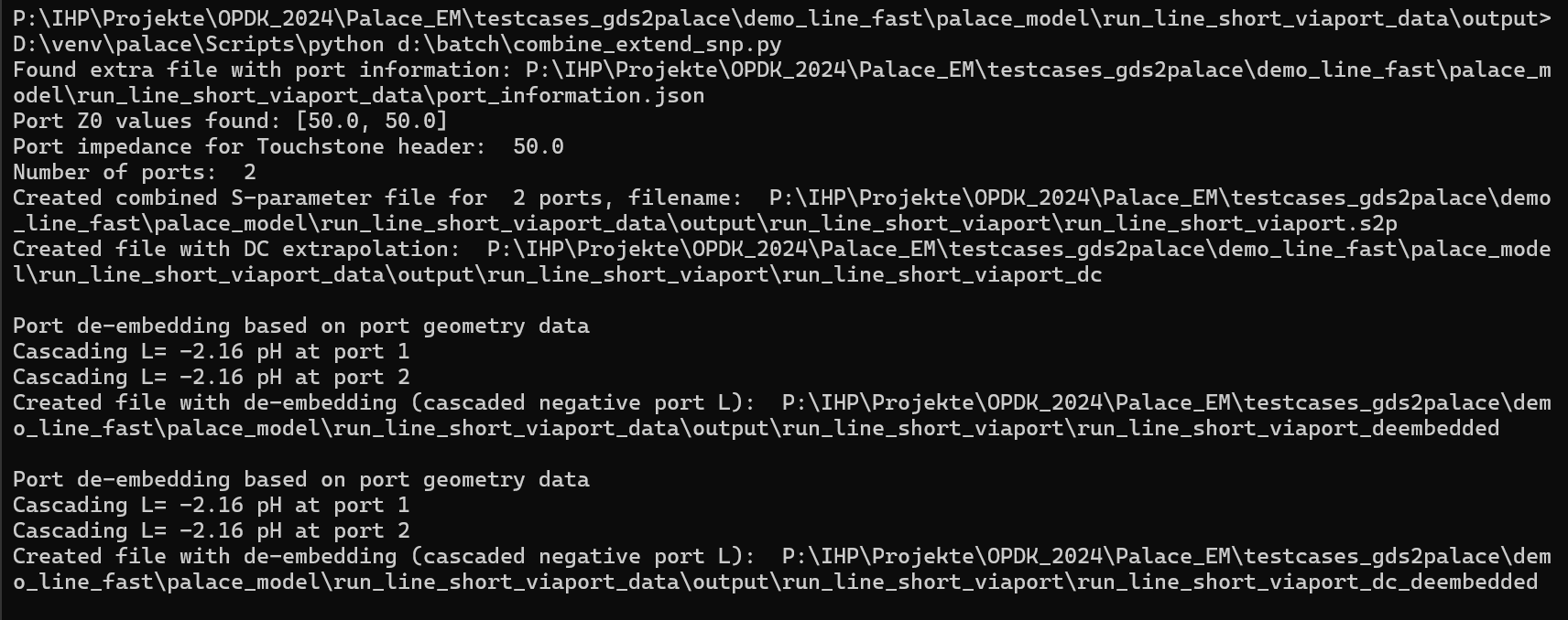
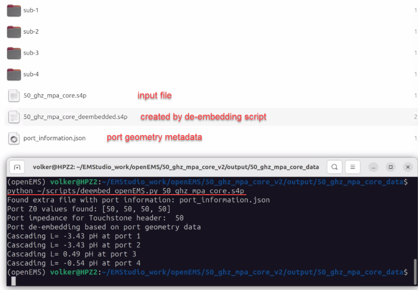
When running combine_snp, the resulting information on calculated parasitic port inductance is also displayed on the command line.
Port de-embedding in openEMS workflow
In February 2026, the workflow for openEMS was updated to create the port_information.json metadata file, similar to the gds2palace workflow.
An external Python post-processing script is provided to create de-embedded S-parameter data from this port metadata plus the original simulation results. This Python script must be started manually, after running the simulation workflow.
https://github.com/VolkerMuehlhaus/openems_ihp_sg13g2/tree/main/scripts
Requirements: Python module scikit-rf must be installed to use this de-embedding script.
Lumped model and SPICE model extraction
Open source circuit simulators don’t support the use of S-parameters for transient simulations, and Harmonic Balance simulations are not always easily available.
To overcome this limitation, we provide two alternative solutions in the IHP EM solver ecosystem:
For some topologies, a physical lumped model can be extracted from the S-parameter data.
Black model mathematical model fit can be applied if no lumped model exists.
Python code for both approaches is available here, based on the scikit-rf library:
https://github.com/VolkerMuehlhaus/lumpedmodel
Lumped model fit
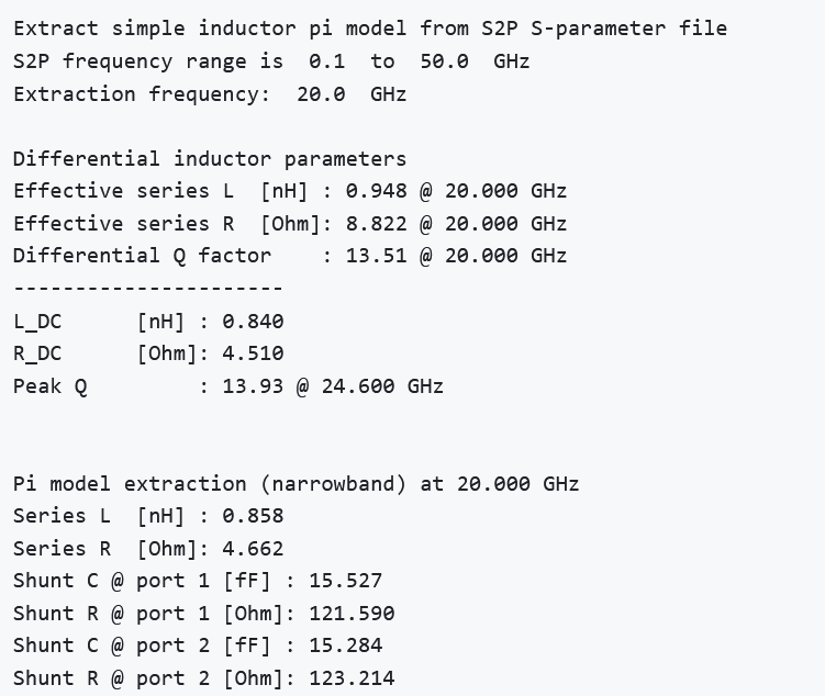
Lumped model extraction provided here is rather simple and exact only narrow band, but it is a robust solution and guaranteed to be well behaved and numerically stable at all frequencies.
These lumped model extraction codes and documentation are available here:
Inductor (two port, no center tap) from S2P data: https://github.com/VolkerMuehlhaus/lumpedmodel/tree/main/pi_from_s2p
MIM capacitor from S2P data: https://github.com/VolkerMuehlhaus/lumpedmodel/tree/main/mim_from_s2p
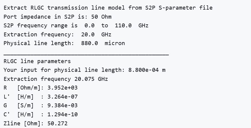
Transmission line from S2P data, resulting in RLCG values: https://github.com/VolkerMuehlhaus/lumpedmodel/tree/main/rlgc_from_s2p
These extraction tools provide circuit model values (no file!) which you can use in qucs-s or other tools.
Transmission line extraction giving data for RLCG model:
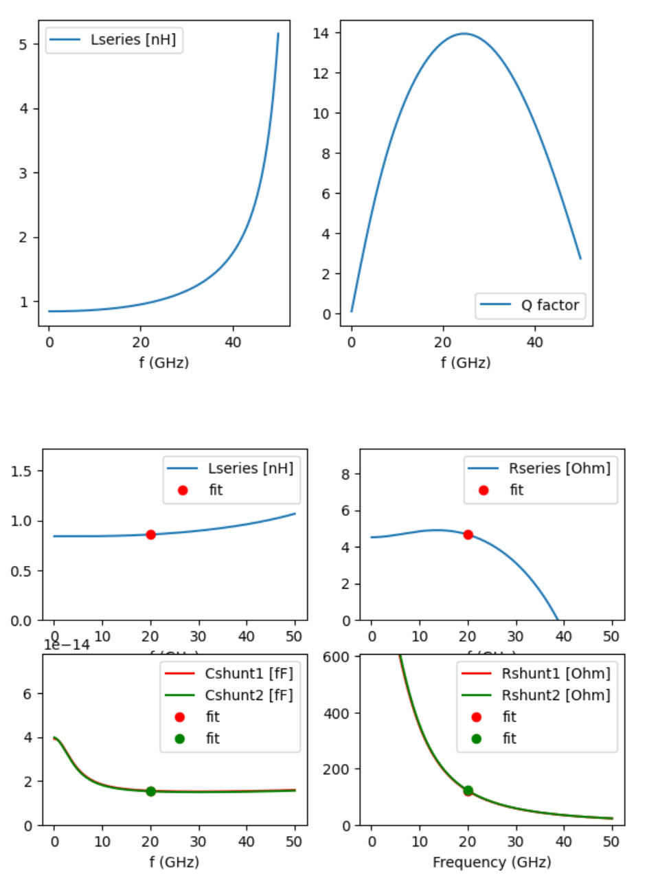
For inductor and MIM extraction, you also get a plot with the model response compared to your original input data.
Black box vector fit
This approach was motivated by testcases and examples from Dietmar Warning of IHP.
The user needs to specify the S-parameter file and (optional) a parameter for the number of poles, which represents the complexity of the transfer function used to fit the data. If the user does not specify a value for model order, this will be found automatically.
The code is not limited to a specific number of ports, but only ports 1 and 2 are shown in the response plot of the fitted data.
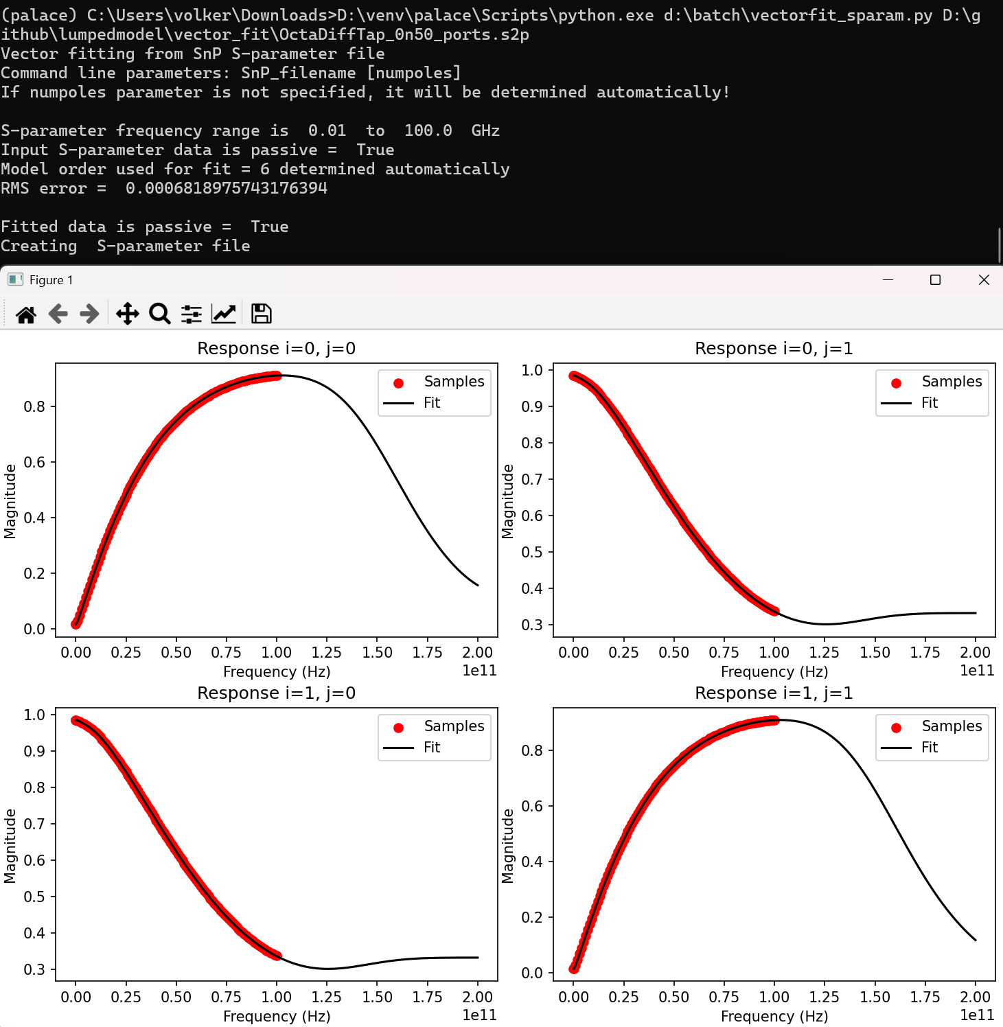
The output created by this code is a netlist with file extension *.sp
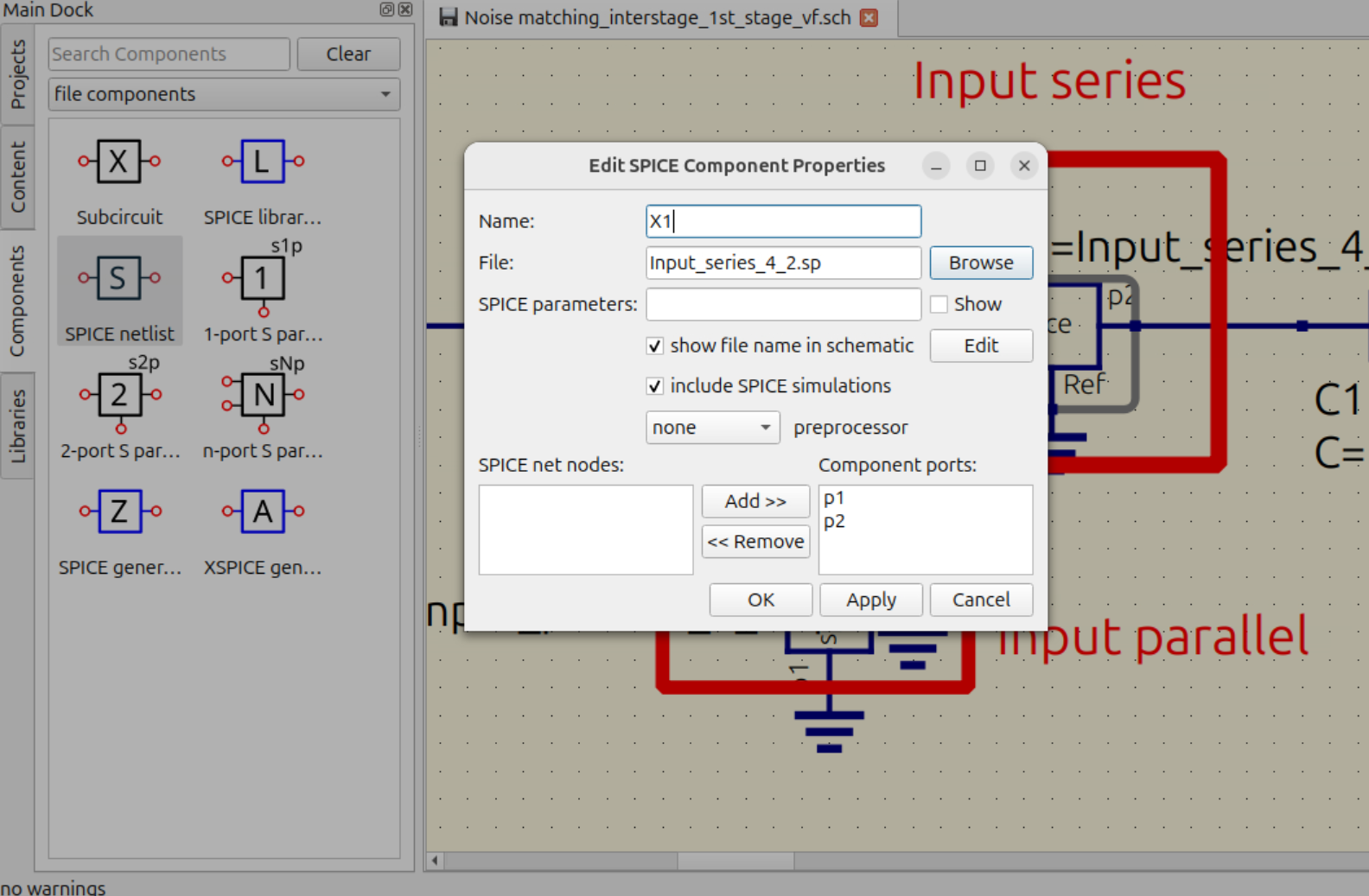
In qucs-s, you can include this netlist using the „SPICE netlist“ component from the file components palette.
Viewing S-simulation results
Some examples for gds2openEMS include result plot in the model code, but for gds2palace this was removed to keep the simulation code clean and simple. Similarly, the setupEM graphical user interface does not plot results, it just creates S-parameter output files.
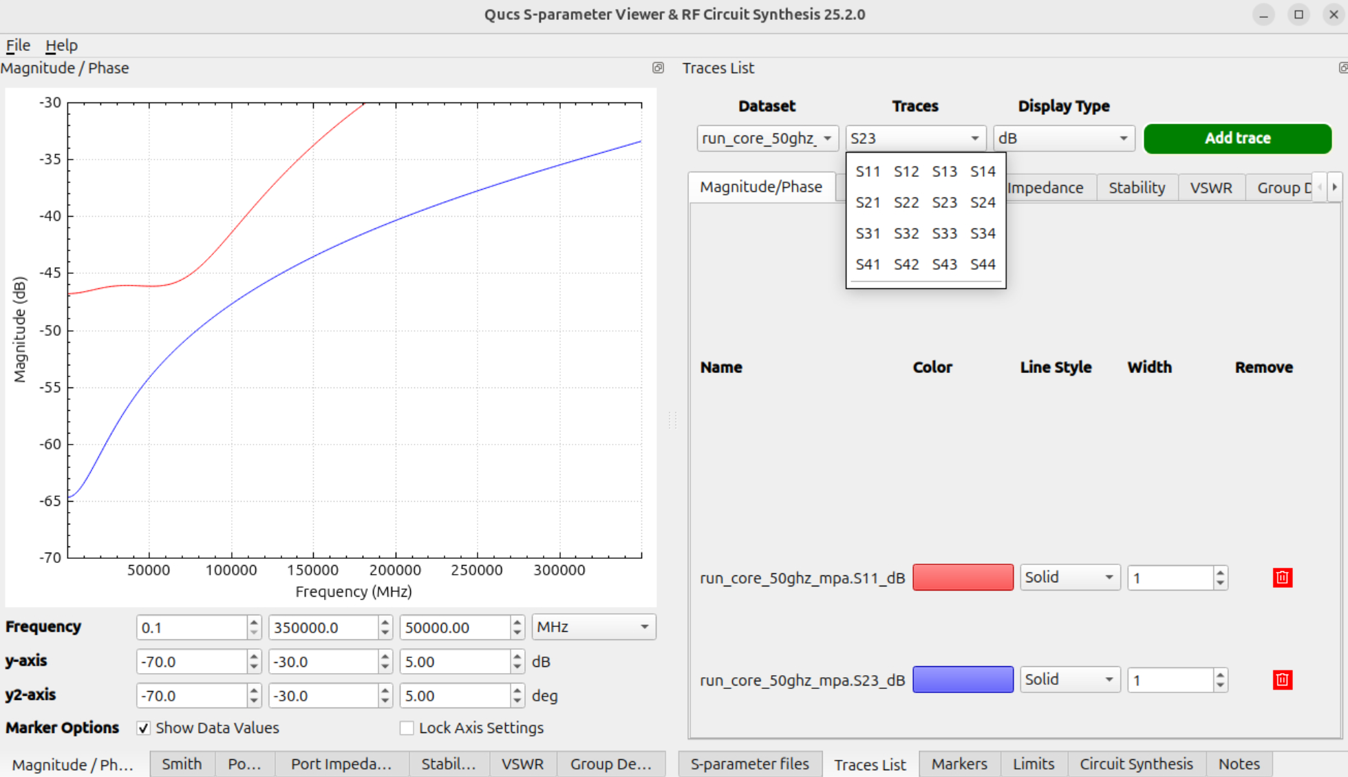
S-parameter viewer in qucs-s
One solution to visually check S-parameter files is the viewer built into qucs-s. This tool can also be used to compare data from multiple files. It can be started from „Tools > S-Parameter viewer & RF circuit synthesis“ in the qucs-s main menu.
Python script „plot_snp“
plot_snp is a Python script that reads one or more S-parameter files with any number of ports (*.s*p) and plots magnitude (dB) and phase of all selected parameters.
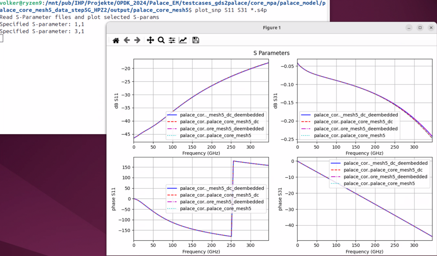
To run the inductor plot and analysis, specify the *.snp file(s) and the requested S-parameters as commandline parameter. Order does not matter.
plot_snp is available at
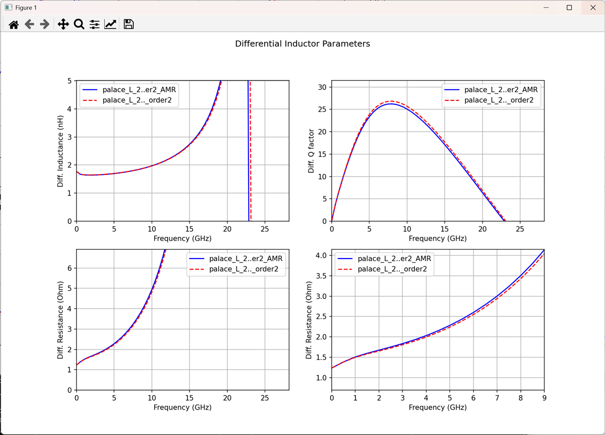
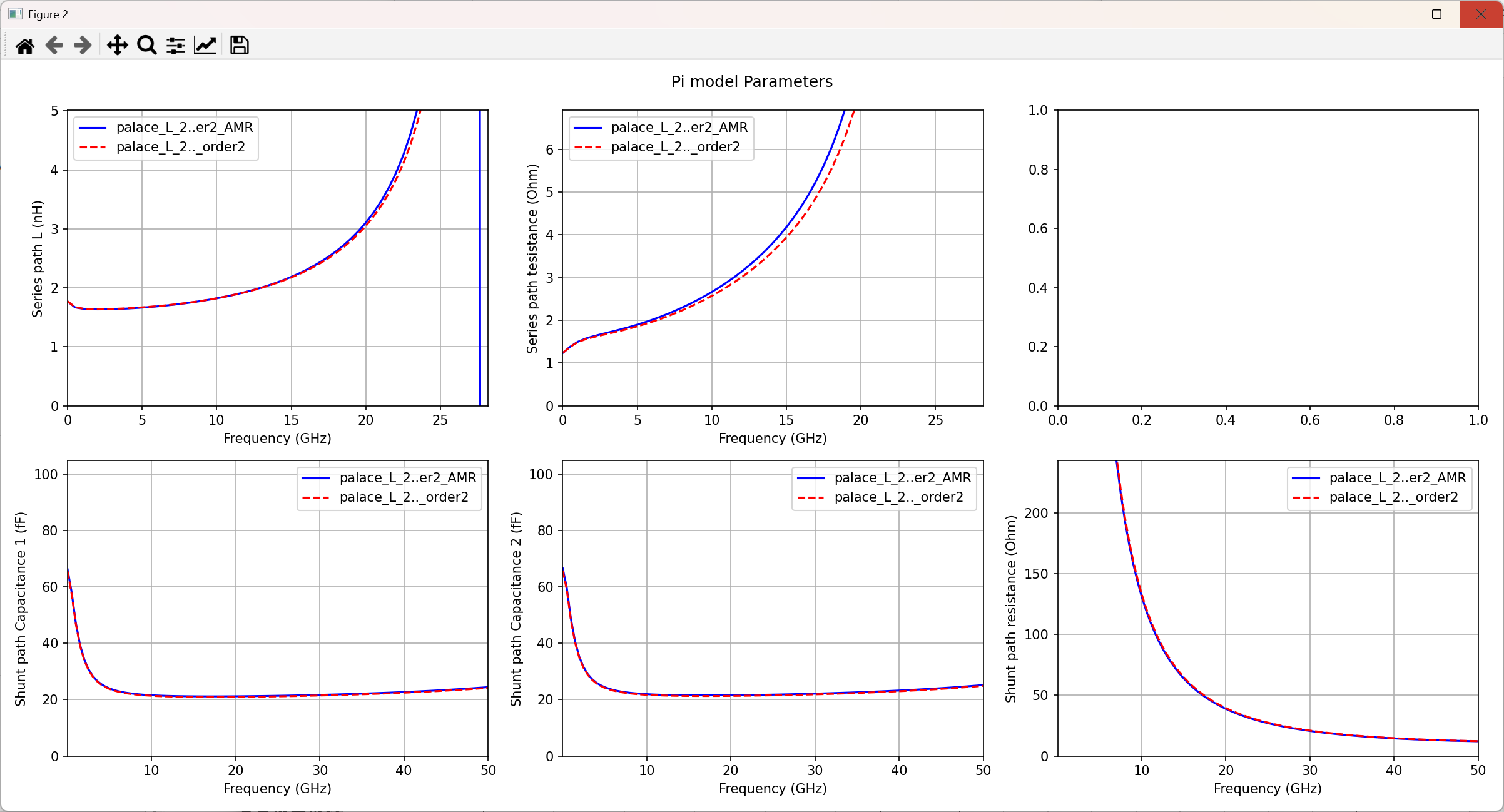
Python script „plot_inductor“
plot_inductor reads S-parameter data with 2 ports (*.s2p) for an RFIC inductor and plots the differential mode (symmetric) effective L, Q and R over frequency.
It support plotting multiple files, and to debug the reason for possible differences, the tool plots the extracted effective series and shunt path elements over frequency. This is really useful to see, for example, if the reason for a difference in Q factor is located in series path or shunt path loss.
https://github.com/VolkerMuehlhaus/plot_inductor
GDSII geometry cleanup prior to simulation
Layouts are usually simple and clean in the initial design phase, but simulating a „final“ layout that was already prepared for tape-out with density rules etc. can be a challenge.
The picture below shows some typical details that would blow up the EM simulation model:
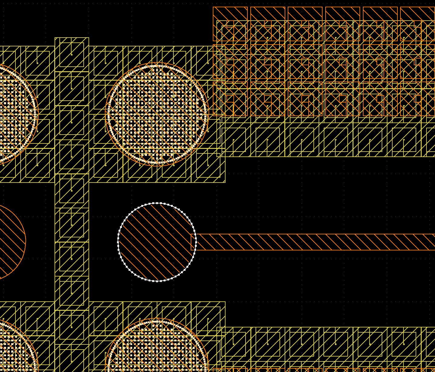
1) To fulfill metal density rules, larger areas have been created as an array of squares with hole inside. This hole does not really matter for EM results, but it will lead to additional mesh cells and slow down mesh generation and simulation.
For openEMS, the value of refined_cellsize can efficiently be used to skip small detail, but still those edges will slow down the edge detection while meshing. For Palace, such small detail will all be included in mesh and it is absolutely required to remove these irrelevant details.
2) On layer TopMetal2 shown as orange boxes on the top right side, and many other layers hidden here, the layout includes unconnected (floating) metal boxes that are solely used to fulfill density rules. Unlike auto-generated dummy metal fill, this “man-made” dummy metal fill is on purpose “drawing“ and can’t be skipped by its purpose (data type).
3) Especially for pads, there is a massive amount of vias located in via arrays at rather large spacing. We can’t simplify increase the distance for via array merging in the gds2palace or gds2openEMS scripts, because that is a global setting and might also create unintentional short between adjacent via stacks.
4) In the case shown here, the pads for copper pillar are round, which is represented in GDSII as a polygon with many vertices, resulting in over-meshing at these polygons, wasting simulation time.
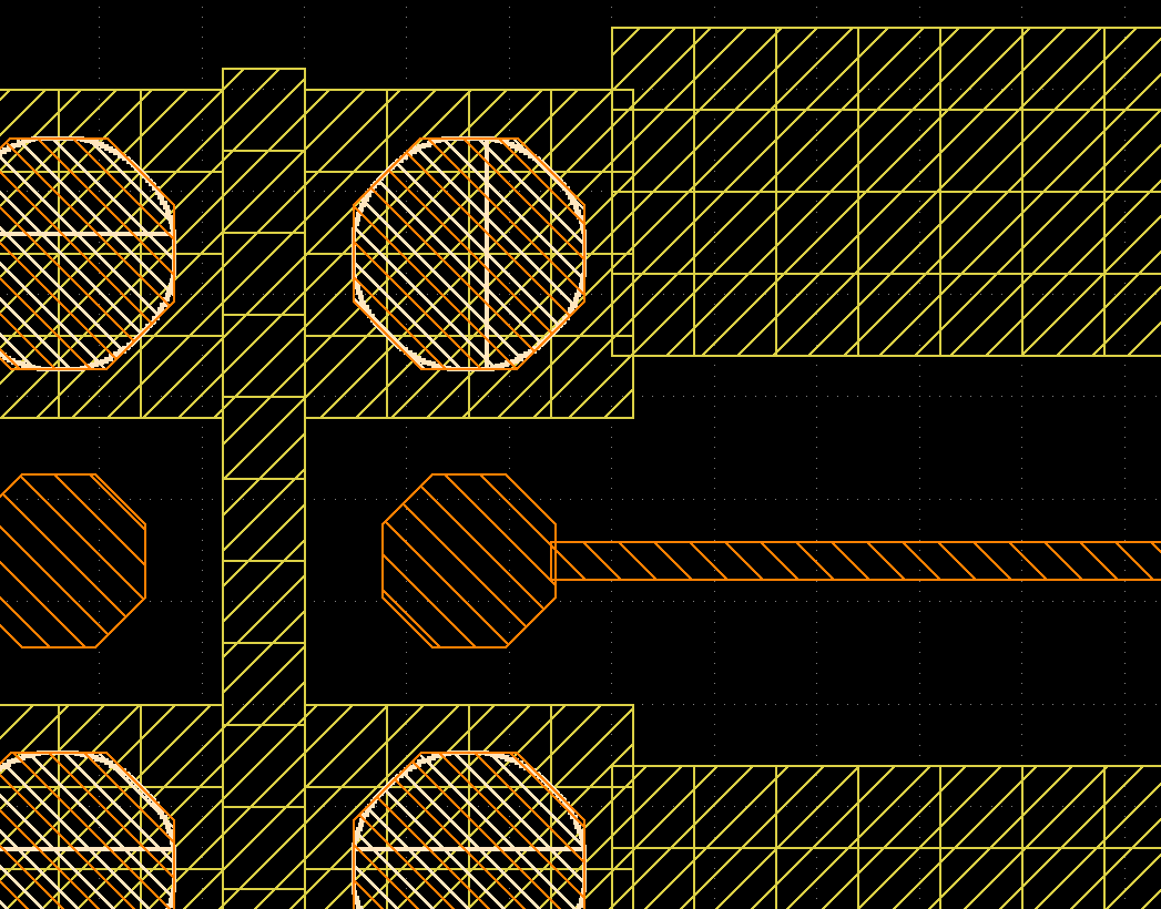
To solve these issues and create a more simulation-friendly layout, a collection of tools is provided at https://github.com/VolkerMuehlhaus/gds_prepare_for_EM
gds_removefill
This tool will check for unconnected (floating) metal fill on purpose drawing, and remove this. By default, the size limit for removing these floating polygons is 1 to 40 microns.
gds_simplify
This tool will check for metals with square shape and square hole inside, which are typical for man-made tweaks to fulfill metal density rules. These polygons are replaced by solid squares with no hole. Also, the tool will check for circle-like polygons, and replace them by an octagon, which is more effiently simulated in the gds2palace workflow.
gds_prepare_for_EM
This all-in-one tool will combine multiple preprocessing steps:
STEP 1: remove cutouts in the hierachical design, don’t flatten at this stage. Do this on metal layers (not via layers, not EM port layers)
STEP 2: via array merging, this also flattens the design hierarchy. Clip merged via arrays to metal boundary above/below, to avoid creating bridges across gaps.
STEP 3: remove floating metals that are not connected to anything, with size in a range
STEP 4: replace circle-like polygons (from metal or result of via array merging) by octagons
Starting from the example above, the resulting cleaned and simplified GDSII then looks like this:
Some example simulations
This chapter showcases some simulation examples using the openEMS and Palace workflow for IHP SG13G2 OPDK.
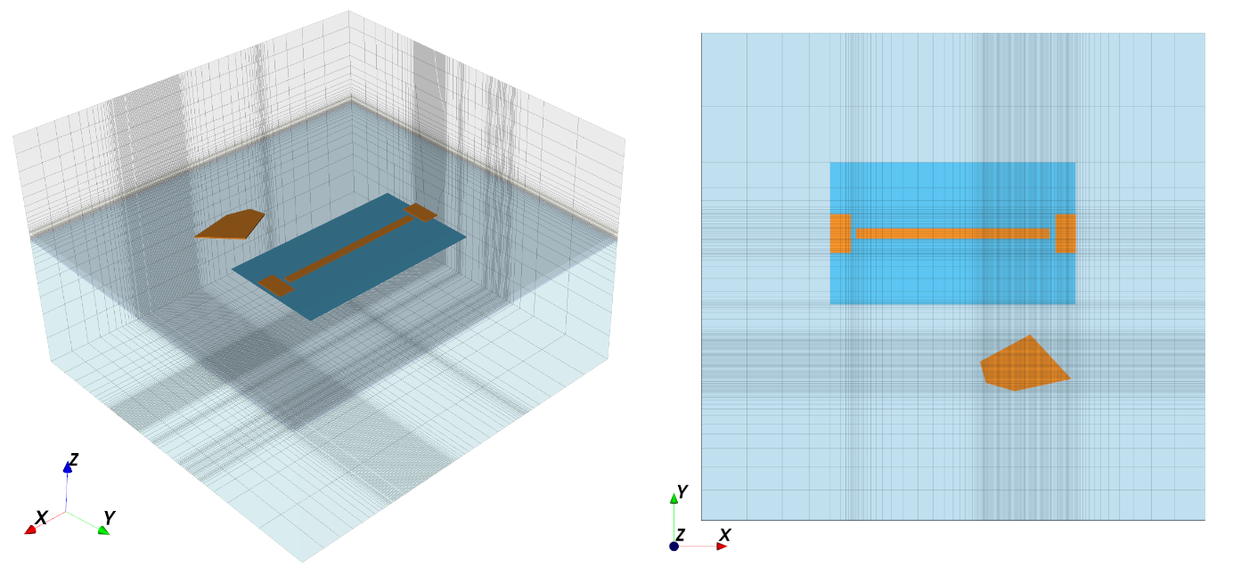
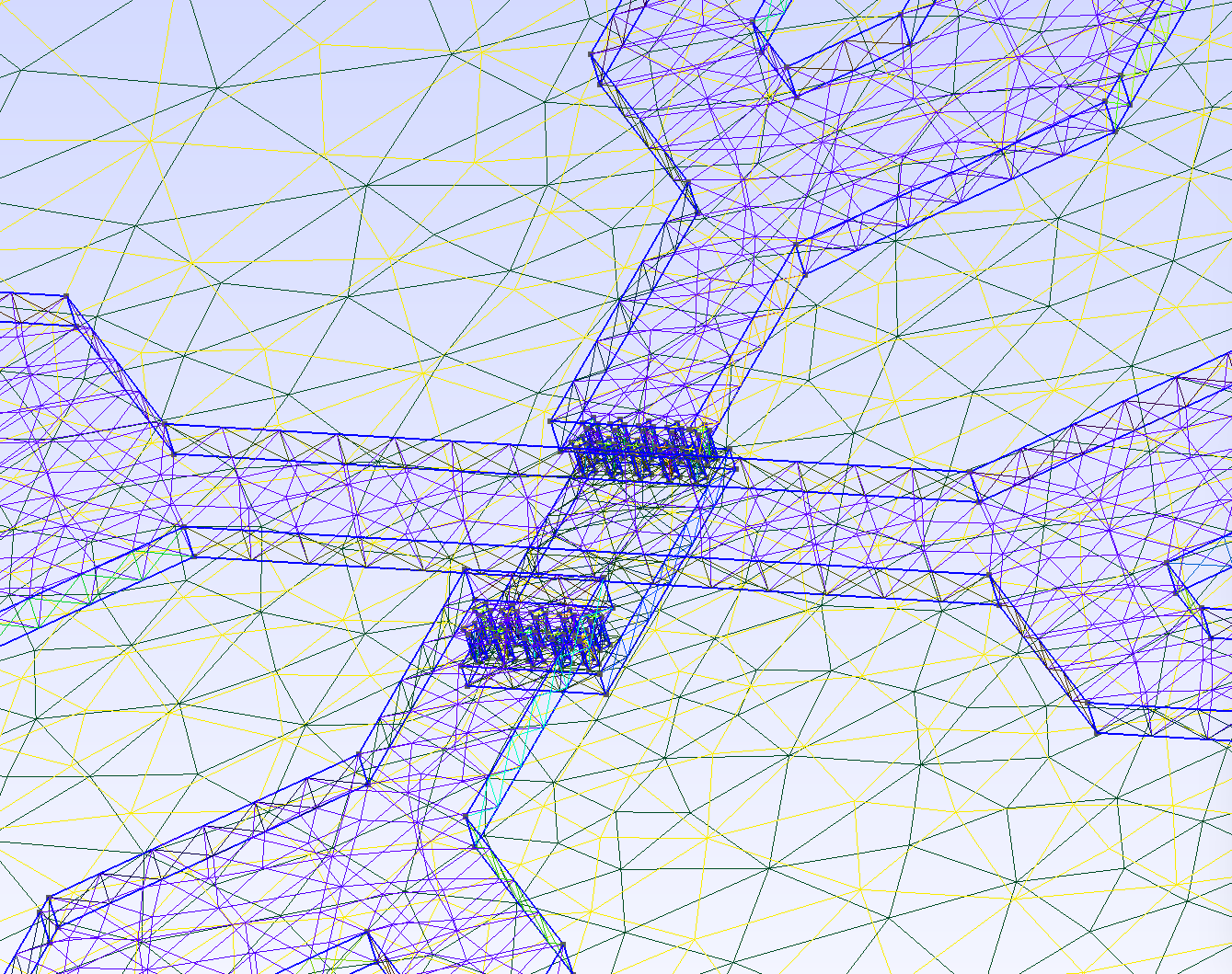
mpa_core
This is an example from IHP Analog Course. The layout has 2 via ports for input/output and 2 in-plane ports where the transistor is connected. Design frequency is 60 GHz, simulation frequency range is 0 to 350 GHz.
OpenEMS simulation
Boundary condition is PML4 absorbing boundary on all sides except for the bottom below the silicon where PEC perfect conductor is defined.
On a Ryzen 5950X with Ubuntu, at refined_cellsize = 0.5 micron each port excitation requires approx. 75 seconds at an average speed of 350 Mc/S FDTD speed. The solver selects 4 cores to run this model (with 16 cores available on that machine). Mesh size is 127 x 109 x 61 cells = 844k FDTD cells. Required RAM for the solver is around 1 GB. Total simulation time for this model with refined_cellsize=0.5 is 4 x 75 seconds = 300 seconds = 5 minutes.
For comparison: if we reduce refined_cellsize from 0.5 micron to 0.3 micron, mesh size grows to 1.9M FDTD cells and due to the smaller minimum cell size, the FDTD timestep also decreases, so that many more FDTD cells must be solved over more total timesteps. The solver chooses to run on 3 cores in this case. Required RAM for the solver is around 3 GB. Total simulation time for this model with refined_cellsize=0.3 is 4 x 220 seconds = 880 seconds = 15 minutes.
This shows how mesh count and minimum mesh cell size influence the openEMS simulation time. If the model has no small geometry features or gaps that must be resolved, and loss from skin effect must not be resolved with highest precision, choosing a larger refined_cellsize can speed up simulation.
Palace simulation
The Palace model is based on the same configuration, with some required changes for FEM. Frequency range is 0 – 350 GHz in 1 GHz steps, with the DC point internally faked from extrapolating low frequency data at 10 MHz and 20 MHz.
Mesh resolution is set as refined_cellsize=2 micron, for high accuracy. Note that refined_cellsize value can’t be directly compared to openEMS because the entire mesh structure is different for FEM. From experience, it is known that adaptive mesh refinement is not required here.
For the Palace simulation, all via arrays are merged, to avoid wasting mesh cells at small details.
With these settings and refined_cellsize=2 micron, simulation of the full S-parameter over the full sweep range requires 251 seconds.
With a coarser mesh at refined_cellsize=5 micron, simulation of the full S-parameter over the full sweep range requires 146 seconds.
For further speed-up, we can reduce the frequency step from dense 1 GHz steps (=350 steps total) to 5 GHz steps. This speeds up the adaptive frequency sweep by more than factor 2.
Unlike openEMS, we can also use Palace to simulate a single frequency, or a few frequencies, instead of the wideband sweep. This will reduce simulation time by a large amount for those cases where we don’t need wide band sweep data, e.g. during the design phase.
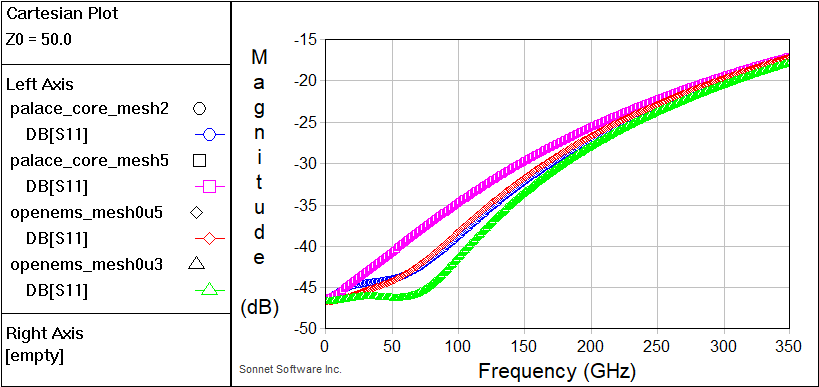
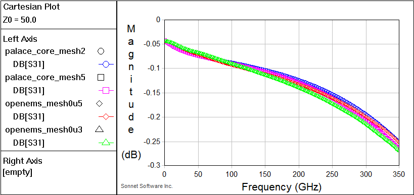
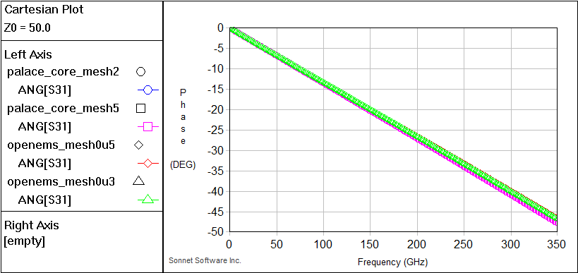
Inductor 400pH @ 40 GHz
This is a typical simulation model where we can see some difference in modeling approach between FDTD and FEM.
Trace width is 5µm and spacing is 4µm, with the Metal1 ground cut out underneath the inductor. To simplify evaluation, the model was only simulated using 2 ports, leaving the center tap floating, but it’s easy to add the 3rd port here.
OpenEMS simulation
Due to the rather wide gap, refined_cellsize=1 micron would be sufficient to sample the geometry without excessive staircasing, but for the metal loss model used in gds2openEMS, we would need smaller values to really mesh into skin depth at the 40 GHz target frequency.
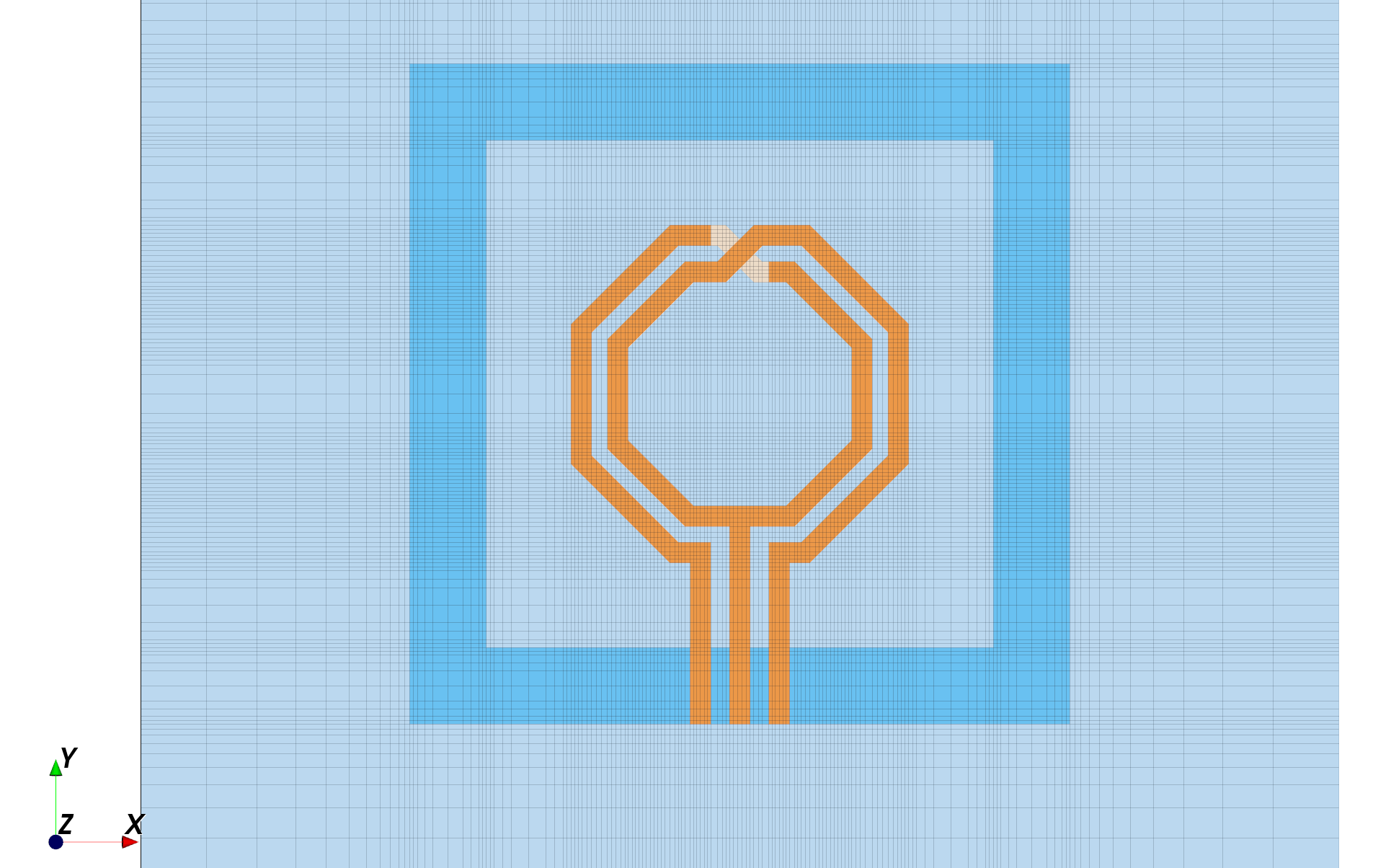
At refined_cellsize=1 micron, the model requires 145x134x42 = 816k FDTD cells and the sweep from 0 – 100 GHz for both port excitations. For this model, the solver selects 8 cores to run this model (with 16 cores available on that machine), with a total simulation time of 150 seconds.
The average FDTD speed is 950 Mcell/s here, because we used PEC boundaries that simulate faster in openEMS than PML absorbing boundaries. These boundaries are placed at 70 micron distance from the Metal1 ground ring. Due to that ground ring, the residual field around the inductor is rather low, so that PEC boundaries at this distance have no effect on simulation results.
If we use refined_cellsize=0.5 micron, to model the metal loss from skin effect more accurately, the model requires 235x206x46 –> 2.22M FDTD cells and total simulation time 720 seconds.
Palace simulation
The Palace metal loss model uses surface impedance to model the metal loss, so that we don’t need to mesh into skin effect.
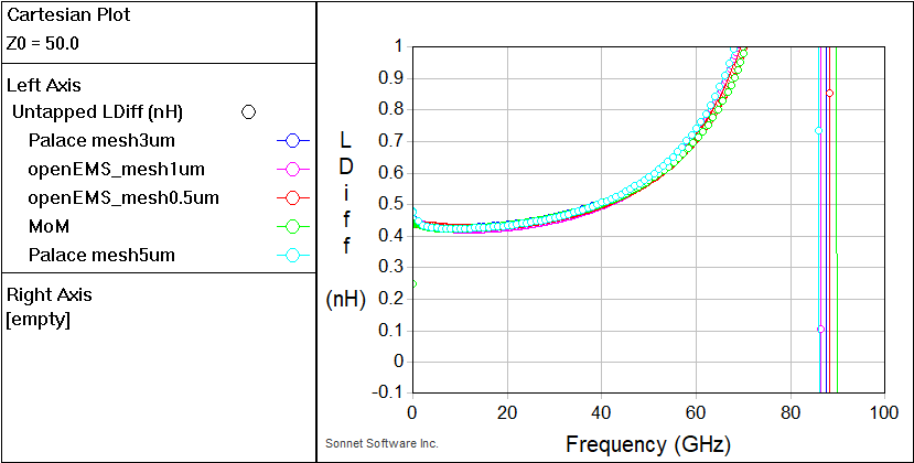
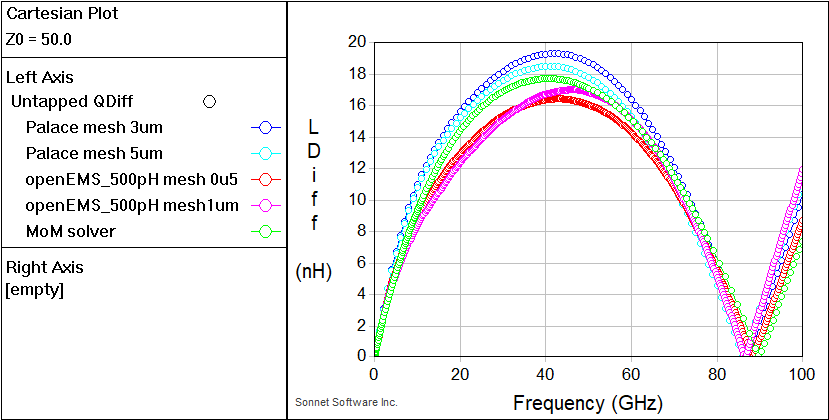
Below is a comparison of results, including data from a Method of Moments solver for reference.
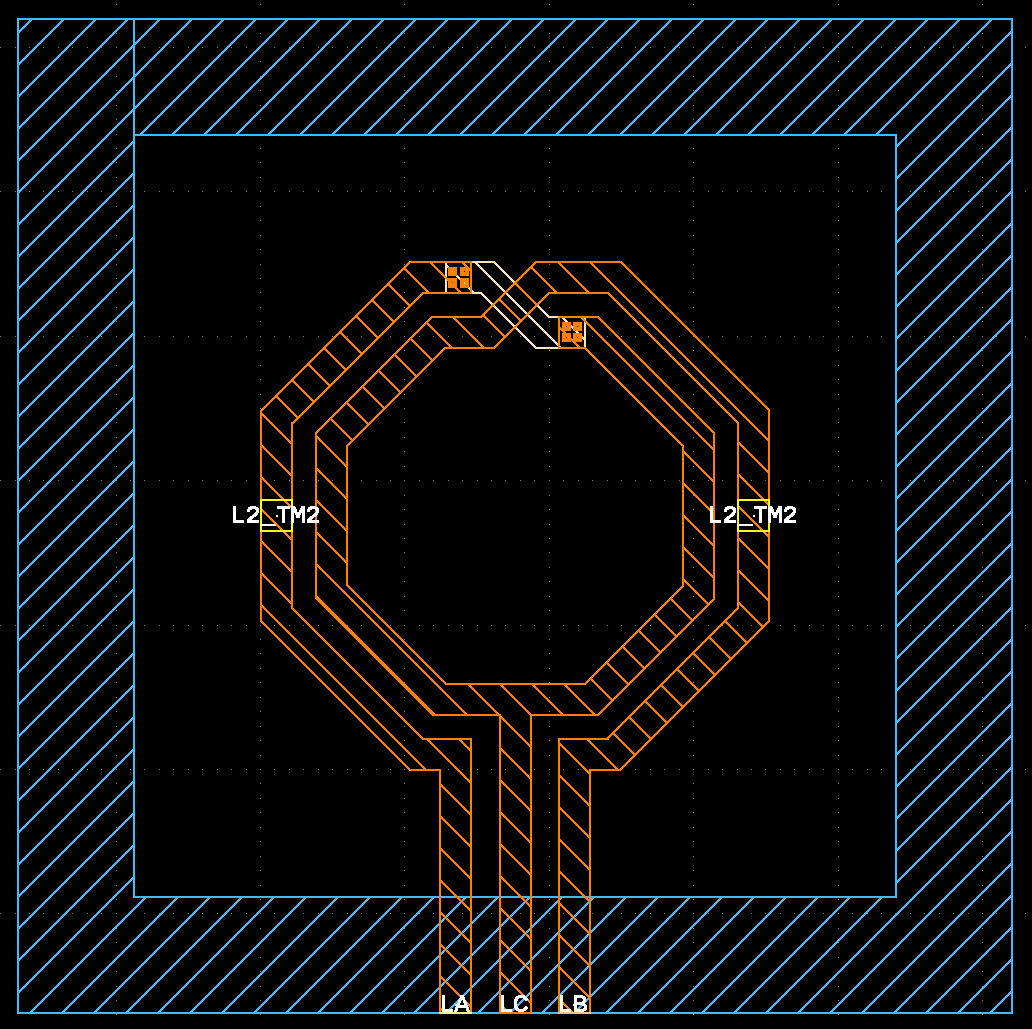
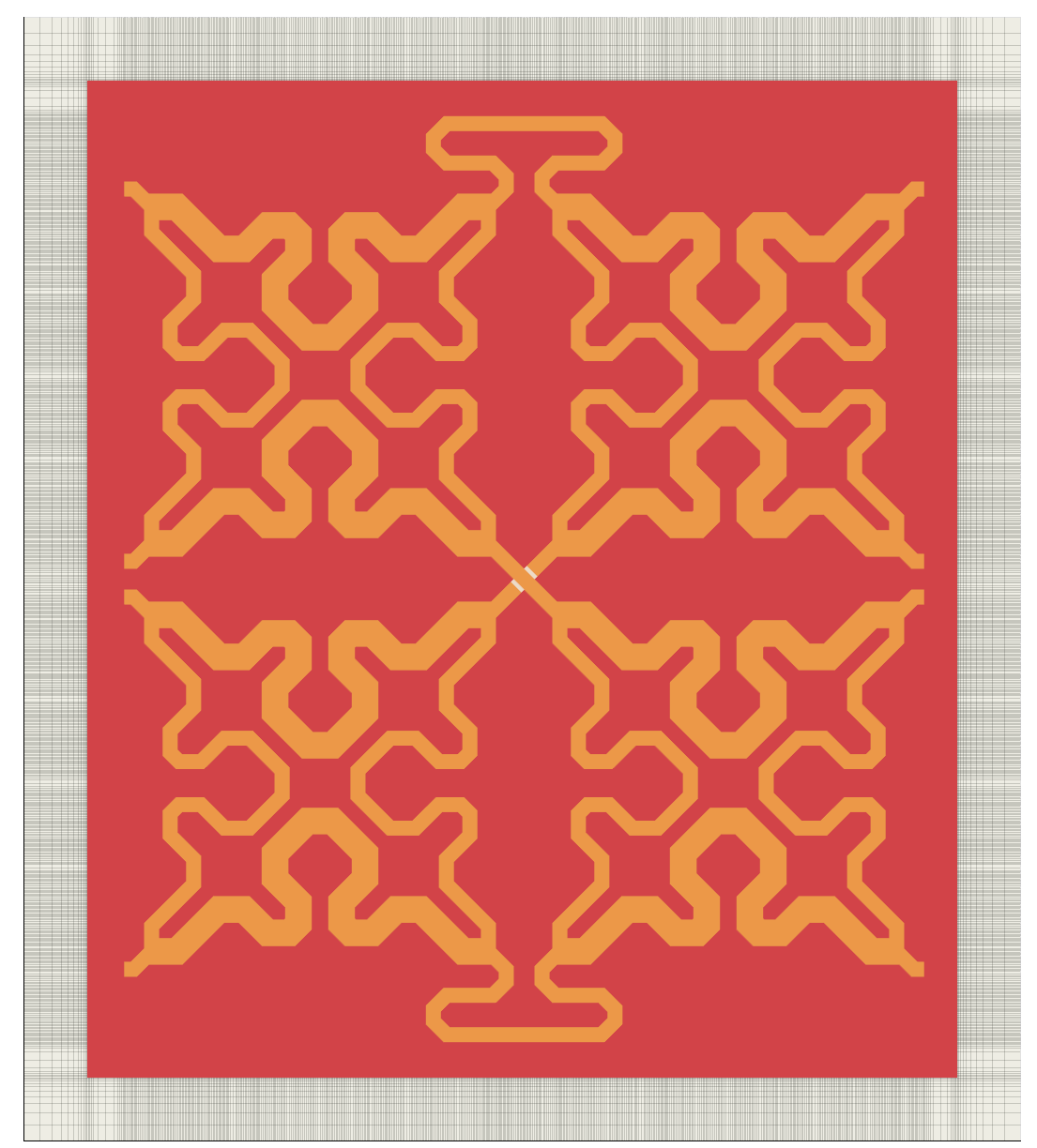
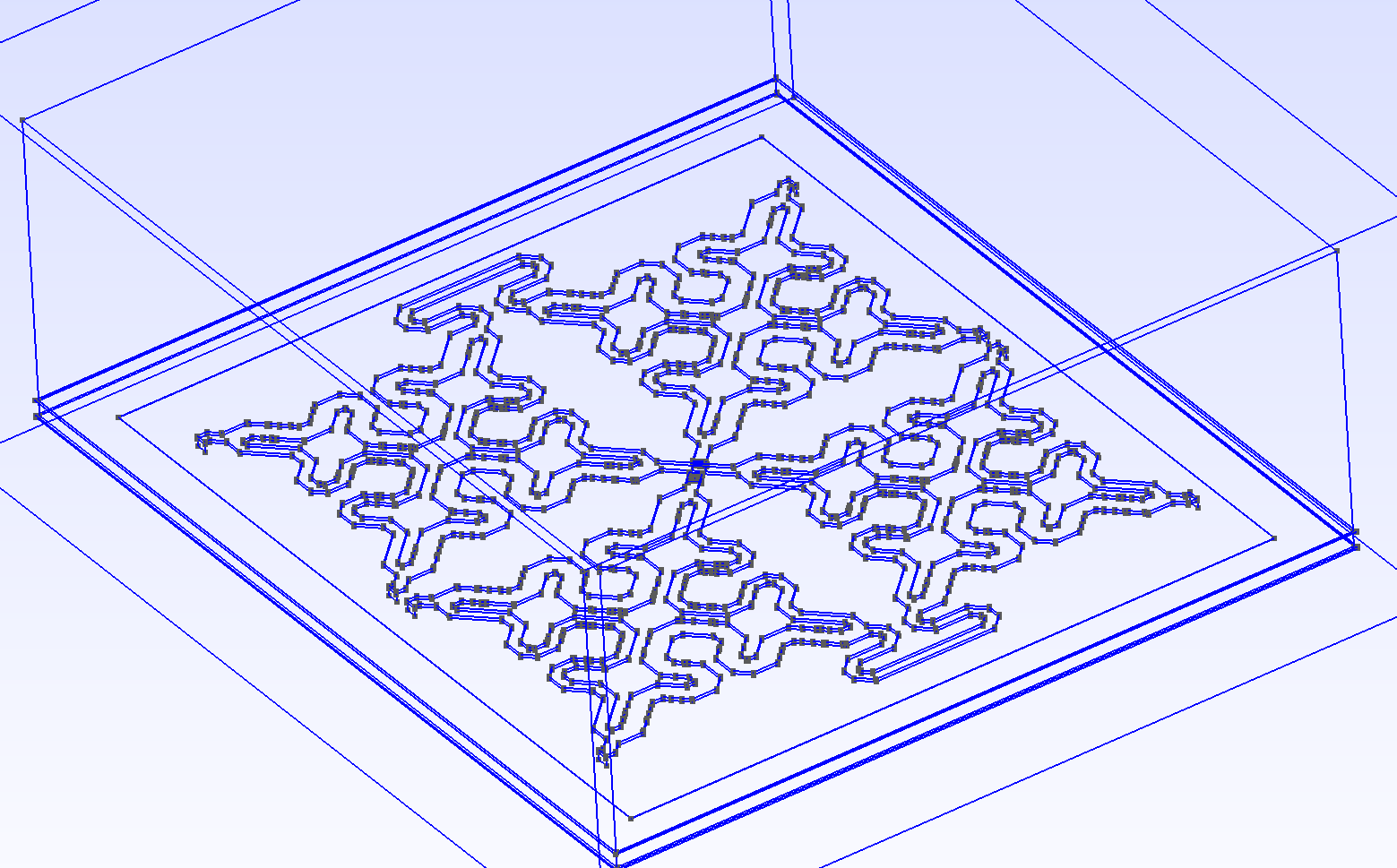
Butler matrix 93 GHz
This simulation investigates a compact on-chip Butler matrix layout for 93 GHz created by Ardavan Rahimian for IHP OpenPDK Tapeout July 2025. The design is available at https://github.com/IHP-GmbH/TO_July2025/tree/main/W_Band_Butler_Matrix_IC
Author of this design: https://ieeexplore.ieee.org/author/37535797800
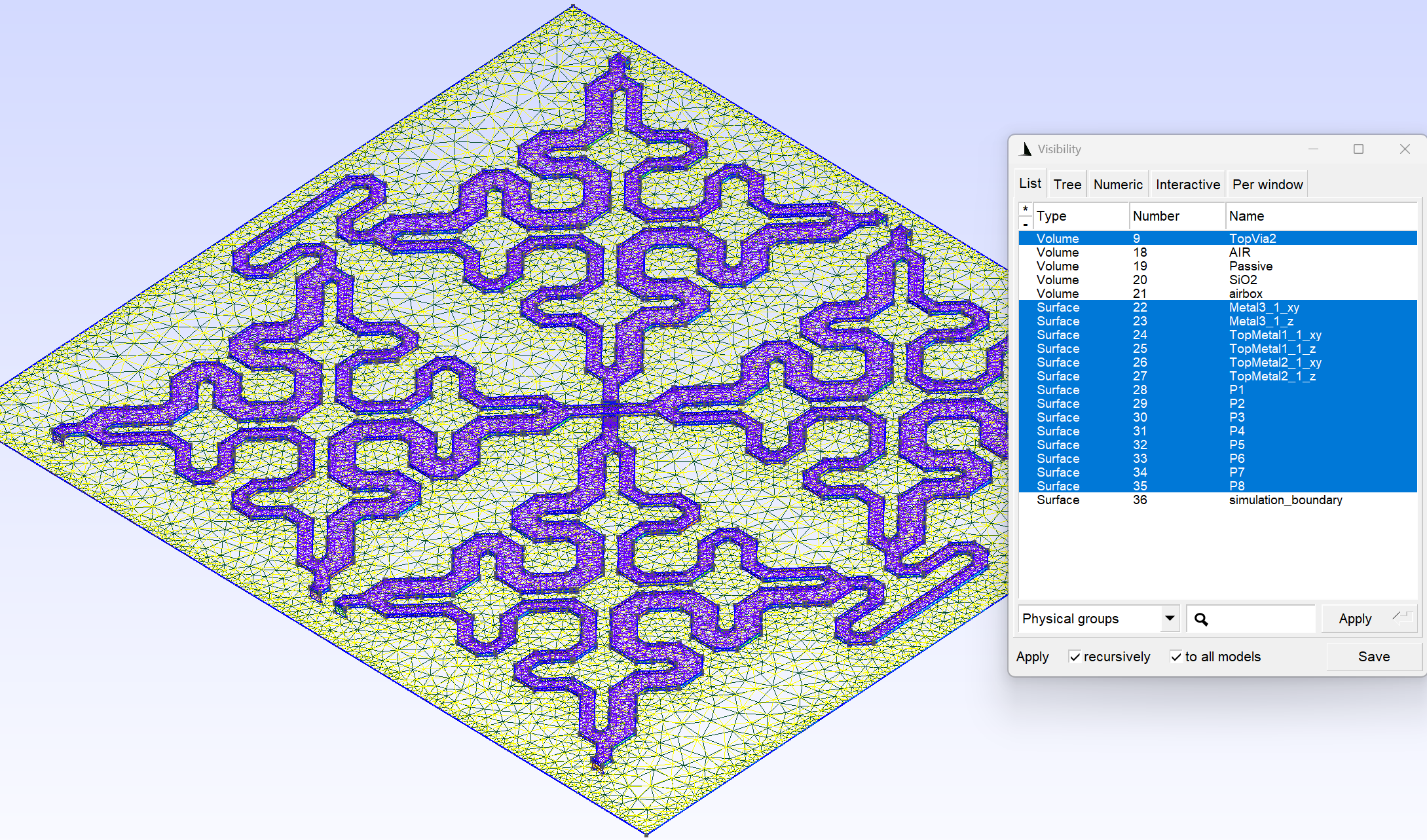
This model has 8 ports, routing is mostly on TopMetal2 over Metal3 ground plane, with a TopMetal1 underpass.
OpenEMS simulation
openEMS at refined_cellsize = 1 micron requires 14.1 million FDTD cells with less than 4 GB RAM. The solver chooses to run on 4 cores in this case. At an average speed of 400 Mcells/s, simulation time for this one excitation was 100 minutes per excitation.
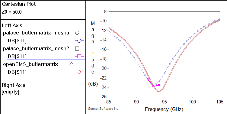
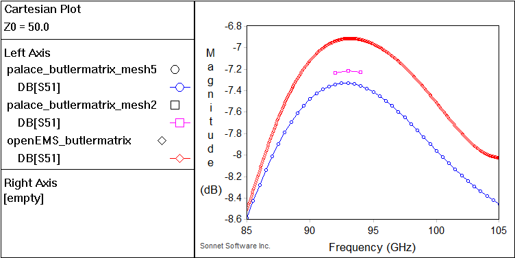
From single port excitation we can get one row of the S matrix, for example S11, S21, S31, S41, S51, S61, S71, S81 over a wide frequency range (used here: 85 – 105 GHz)
To get full S matrix: 8 excitations * 100 minutes = 800 minutes total = 13.3 hours for full S-parameters for the full sweep.
It must be mentioned that the 1 micron cellsize used here is not sufficient to mesh into skin effect at the 93 GHz target frequency, so results might not be accurate for conductor loss.
Palace simulation
In the gds2palace workflow, metal loss is modeled as surface impedance which has skin effect built into the sheet impedance model. This means we don’t need to mesh into skin effect. Also, the FEM mesh uses arbitrary orientation and local mesh refinement, which allows a larger value of refined_cellsize.
Here, an initial value of 5 micron was used, and a refined value of 2 micron was used to verify that result at some selected frequencies.
Different from openEMS FDTD, the FEM simulation is done in frequency domain, so that the number of frequency points has a strong effect on simulation time.
Here is a strategy that might be used for such large models:
Run an initial sweep over some frequency range, but use “fast“ mesh settings, e.g. larger refined_cellsize or FEM basis function order 1 (“faster, less accurate”) instead of 2 (“most accurate”). This is to check if there are any fundamental issues with the model, like gaps or wrong port polarity.
If the “quick & dirty“ sweep looks good, run the regular simulation sweep, using FEM basis order 2. When a reasonable refined_cellsize is used, you usually don’t need to enable adaptive mesh refinement.
To verify the accuracy of results, you could to run a single frequency simulation at an even smaller value of refined_cellsize. This can be used to check for possible differences in results, and decide if the finer mesh is really needed.
Of course, another alternative is to use adaptive mesh refinement (AMR) and let the solver do multiple runs. The convergence criteria in gds2palace are set so tight that AMR will usually run all the specified mesh refinements, at 70% increase in mesh cells per iteration, over all specified frequencies. This is often slower than starting from a finer initial mesh size without AMR.
For the model shown here, gds2palace at refined_cellsize = 5 micron and regular settings (FEM basis function order 2) requires ~ 4 minutes for one frequency and one port excitation.
For the full 8 port S-matrix over the 85-105 GHz range in steps of 0.5 GHz, it takes 4 hours at refined_cellsize = 5 micron, using 2.8 M degrees of freedom. RAM required for this simulation was ~ 23 GB. The frequency sweep used adaptive frequency sweep, so that not all individual frequencies needed to be simulated.
Below, some simulation results are compared, but of course this is not a full evaluation of the 8-port model.
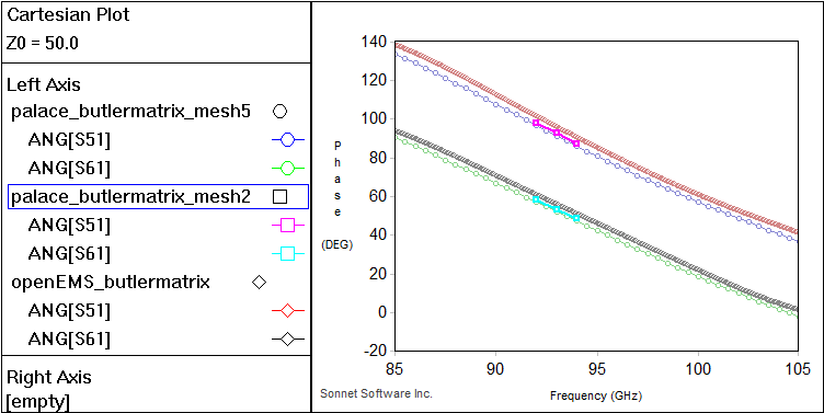
It should be noted that in Palace, simulating all ports will require extra simulation time compared to single port excitation. To verify phase offset between outputs, one fast simulation strategy might be to analyze a single port excitation at a single frequency first. For example, from port 1 excitation we can get S11,S21,S31,S41,S51,S61,S71,S81 which might be already useful here.
At refined_cellsize = 5 micron, this only requires ~ 4 minutes for one frequency and one port excitation, compared to 4 hours for full S-matrix with a detailed sweep over the 85-105 GHz band.
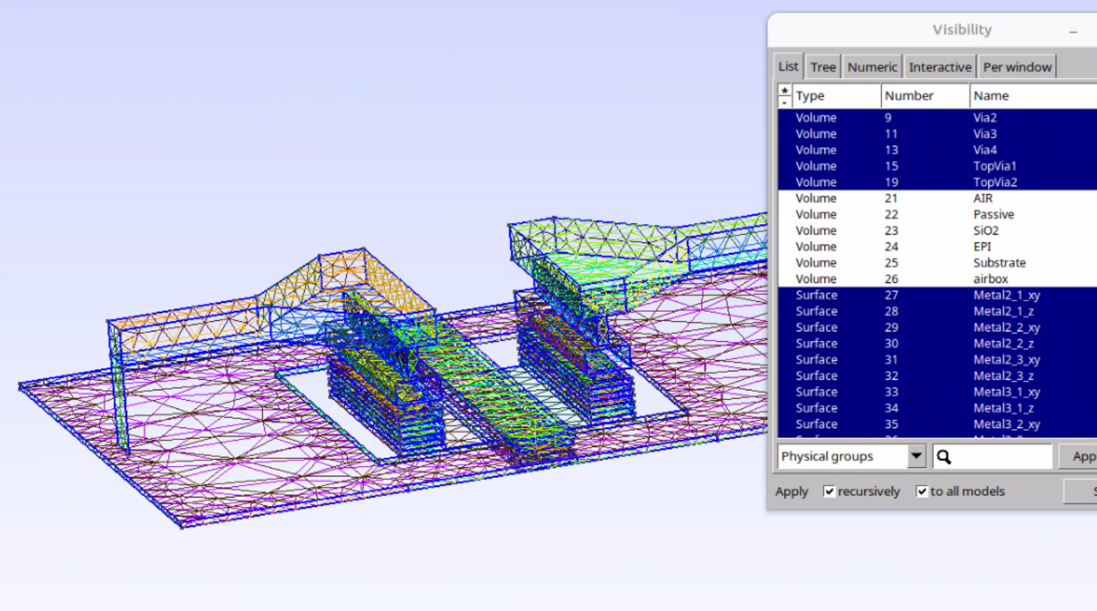
Stacked Technology using openEMS flow
The model below shows an early example of a multi-technology configuration simulated using the openEMS flow.
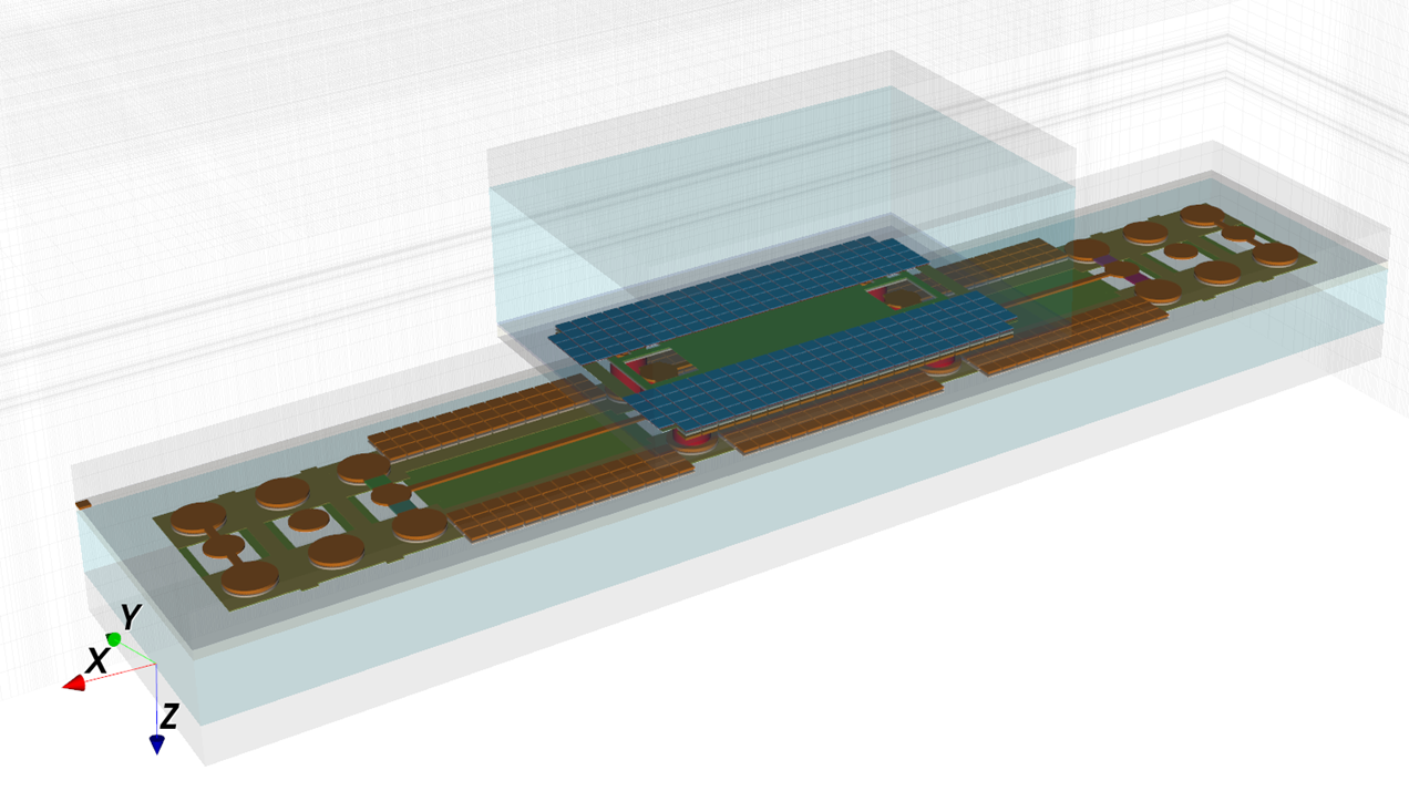
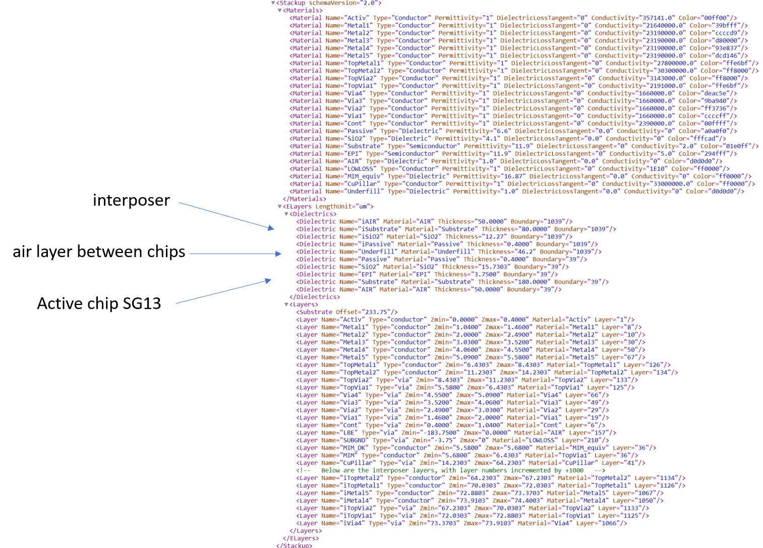
The model code and the stackup file were extended to handle a finite size of the dielectric layers (oxide, passivation and silicon) so that we can stack multiple chips of different size. A single composite XML stackup file was created that combined both technologies into one stackup.
Why openEMS? There are many unconnected floating metal elements used in this layout to fulfill metal density rules, and the FDTD method used in openEMS can handle this large amount of metal quite well, as long as there is no excessive amount of diagonal or curved lines to be meshed.
In FDTD, the mesh lines extend through the entire simulation domain. Once we have meshlines for metal on one layer, extra metal stacked on other layers above or below in that area will not increase model complexity, it doesn’t matter if the material modeled there is oxide or metal.
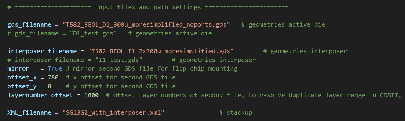
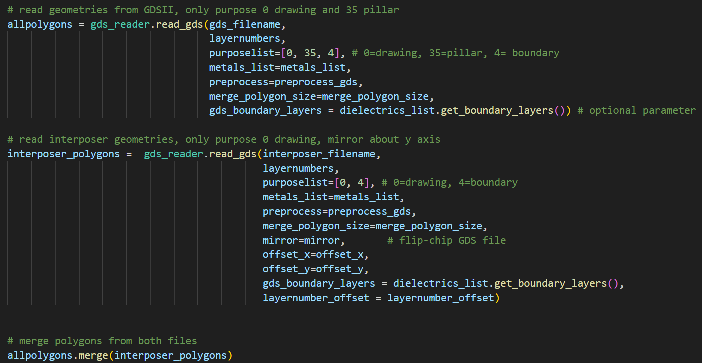
The layout of both parts (active die and interposer) come from separate GDSII files and an additional difficulty in this case was that both use the same layer number range. To resolve this, all layers of the upper chip were offset when reading the GDSII file, so that they have a unique layer number internally.
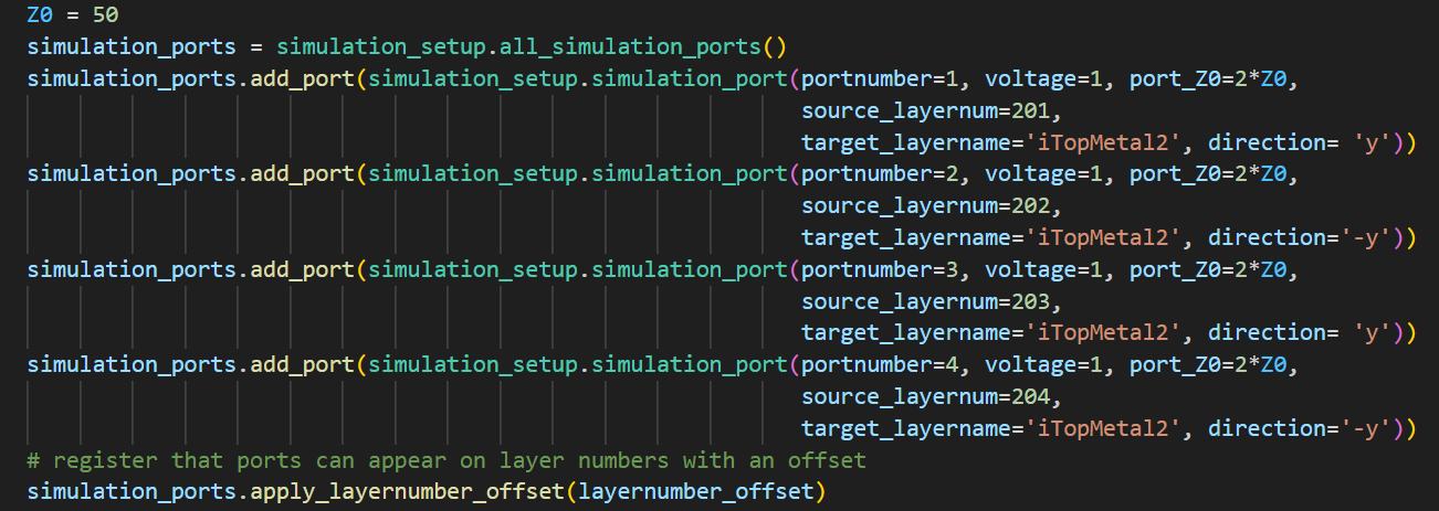
Below are some snippets from the model code, where two GDSII files are defined and one of them is mirrored and shifted, with layer number offset:
Layer number offset applied to ports:
Actual import of GDSII files and combining them into one internal layout data struture:
The simulation for port 1 excitation (single path) with frequency range 0-110 GHz took 90 minutes on a Ryzen 5950X computer, with a mesh of 659 x 184 x 80 cells.
This model was simulated with refined_cellsize=2 micron, which is larger than skin depth, and some inaccuracy is expected for conductor loss. Smaller mesh size would be more accurate for insertion loss, but also take more simulation time.
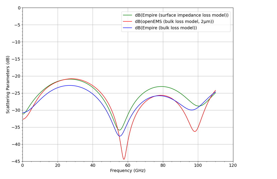
Comparison of S11 results to commercial FDTD solver Empire XPU, which offers two different conductor loss models:
bulk loss model similar to openEMS, where we need to mesh into skin effect
surface impedance model with built-in skin effect correction (similar to Palace)
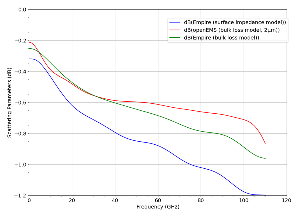
Comparison of S21 results to commercial FDTD solver Empire XPU, which offers two different conductor loss models:
bulk loss model similar to openEMS, where we need to mesh into skin effect
surface impedance model with built-in skin effect correction (similar to Palace)
The model was not simulated using gds2palace because the large amount of metal edges would cause a really complex mesh with very high RAM requirement. FDTD is more efficient for this.
To simulate this model efficiently using gds2palace, the layout should be cleaned and pre-processed first. Some Python code for that preprocessing was presented earlier in this document.