4.2. RFMOSFET Devices
4.2.1. rfnmos
Device Information
Property |
Value |
|---|---|
Description |
nMOS device with ptap surrounding and special RF model. |
Device Recognition |
Activ, GatPoly, psD (For ptap), text (rfnmos) |
Model Name |
rfnmos |
Layout Cell Name |
sg13g2_pr - rfnmos |
Parameters |
w, l, ng, m |
Netlist Syntax |
MN1 D G S B rfnmos w=1.0u l=0.72u ng=1 m=1 |
Additional Notes |
For RF purposes, you should use l = [0.13:1.0]um and w = [1:6]um (per single gate). |
Parameters Information
Parameter |
Description |
Schematic-View |
LVS-View |
LVS-Comparison |
|---|---|---|---|---|
w |
Transistor width |
✅ |
✅ |
✅ |
l |
Transistor channel length |
✅ |
✅ |
✅ |
m |
Number of transistors (multiplicity) |
✅ |
❌ |
❌ |
ng |
Number of gates |
✅ |
❌ |
❌ |
Tip
The m parameter is implicitly calculated in the layout extracted netlist within the value of the w parameter, which represents the total width.
Example: MN0 D G S B rfnmos w=1u l=1u m=2, this will be recognized as MN0 D G S B rfnmos w=2u l=1u
See Figure 4.1.1 for an explanation.
The ng parameter will be ignored, as the w represents total width of all fingers.
The finger width (WF) is defined as w/ng
Example: MN0 D G S B rfnmos w=1u l=1u ng=2, this will be recognized as MN0 D G S B rfnmos w=1u l=1u
See Figure 4.1.1 for an explanation.
Layout Information (Refer to Layout Layers)
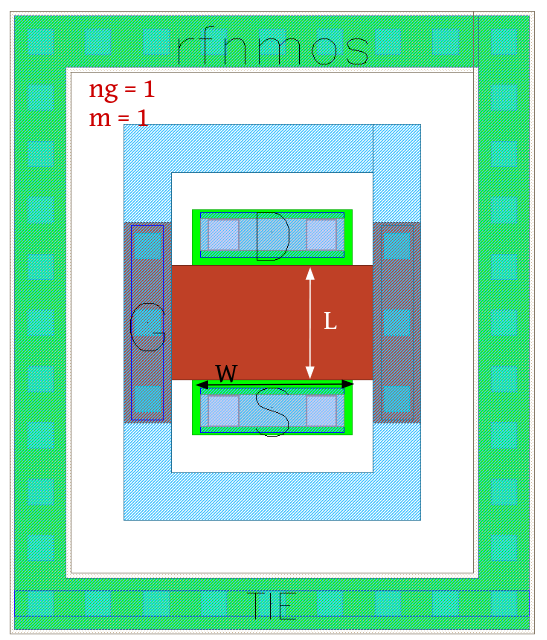
Figure 4.2.1 Layout for RF nMOS-LV transistor
4.2.2. rfnmosHV
Device Information
Property |
Value |
|---|---|
Description |
nmosHV device with ptap surrounding and special RF model. |
Device Recognition |
Activ, GatPoly, ThickGateOx, psD (For ptap), text (rfnmosHV) |
Model Name |
rfnmosHV |
Layout Cell Name |
sg13g2_pr - rfnmosHV |
Parameters |
w, l, ng, m |
Netlist Syntax |
MN1 D G S B rfnmoshv w=1.0u l=0.72u ng=1 m=1 |
Additional Notes |
For RF purposes you should use l = [0.45:1.0]um and w = [1:6]um (per single gate). |
Parameters Information
Parameter |
Description |
Schematic-View |
LVS-View |
LVS-Comparison |
|---|---|---|---|---|
w |
Transistor width |
✅ |
✅ |
✅ |
l |
Transistor channel length |
✅ |
✅ |
✅ |
m |
Number of transistors (multiplicity) |
✅ |
❌ |
❌ |
ng |
Number of gates |
✅ |
❌ |
❌ |
Tip
The m parameter is implicitly calculated in the layout extracted netlist within the value of the w parameter, which represents the total width.
Example: MN0 D G S B rfnmoshv w=1u l=1u m=2, this will be recognized as MN0 D G S B rfnmoshv w=2u l=1u
See Figure 4.1.1 for an explanation.
The ng parameter will be ignored, as the w represents total width of all fingers.
The finger width (WF) is defined as w/ng
Example: MN0 D G S B rfnmoshv w=1u l=1u ng=2, this will be recognized as MN0 D G S B rfnmoshv w=1u l=1u
See Figure 4.1.1 for an explanation.
Layout Information (Refer to Layout Layers)
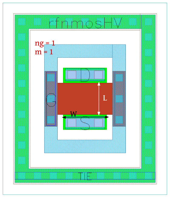
Figure 4.2.2 Layout for RF nMOS-HV Transistor
4.2.3. rfpmos
Device Information
Property |
Value |
|---|---|
Description |
pMOS device with ntap surrounding and special RF model. |
Device Recognition |
Activ, GatPoly, pSD, Nwell, text (rfpmos) |
Model Name |
rfpmos |
Layout Cell Name |
sg13g2_pr - rfpmos |
Parameters |
w, l, ng, m |
Netlist Syntax |
MN1 D G S B rfpmos w=1.0u l=0.72u ng=1 m=1 |
Additional Notes |
For RF purposes you should use l = [0.13:1.0]um and w = [1:6]um (per single gate). |
Parameters Information
Parameter |
Description |
Schematic-View |
LVS-View |
LVS-Comparison |
|---|---|---|---|---|
w |
Transistor width |
✅ |
✅ |
✅ |
l |
Transistor channel length |
✅ |
✅ |
✅ |
m |
Number of transistors (multiplicity) |
✅ |
❌ |
❌ |
ng |
Number of gates |
✅ |
❌ |
❌ |
Tip
The m parameter is implicitly calculated in the layout extracted netlist within the value of the w parameter, which represents the total width.
Example: MP0 D G S B rfpmos w=1u l=1u m=2, this will be recognized as MP0 D G S B rfpmos w=2u l=1u
See Figure 4.1.1 for an explanation.
The ng parameter will be ignored, as the w represents total width of all fingers.
The finger width (WF) is defined as w/ng
Example: MP0 D G S B rfpmos w=1u l=1u ng=2, this will be recognized as MP0 D G S B rfpmos w=1u l=1u
See Figure 4.1.1 for an explanation.
Layout Information (Refer to Layout Layers)
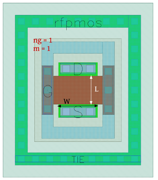
Figure 4.2.3 Layout for RF pMOS-LV Transistor
4.2.4. rfpmosHV
Device Information
Property |
Value |
|---|---|
Description |
pmosHV device with ntap surrounding and special RF model. |
Device Recognition |
Activ, GatPoly, pSD, Nwell, ThickGateOx, text (rfpmosHV) |
Model Name |
rfpmosHV |
Layout Cell Name |
sg13g2_pr - rfpmosHV |
Parameters |
w, l, ng, m |
Netlist Syntax |
MN1 D G S B rfpmoshv w=1.0u l=0.72u ng=1 m=1 |
Additional Notes |
For RF purposes you should use l = [0.40:1.0]um and w = [1:6]um (per single gate). |
Parameters Information
Parameter |
Description |
Schematic-View |
LVS-View |
LVS-Comparison |
|---|---|---|---|---|
w |
Transistor width |
✅ |
✅ |
✅ |
l |
Transistor channel length |
✅ |
✅ |
✅ |
m |
Number of transistors (multiplicity) |
✅ |
❌ |
❌ |
ng |
Number of gates |
✅ |
❌ |
❌ |
Tip
The m parameter is implicitly calculated in the layout extracted netlist within the value of the w parameter, which represents the total width.
Example: MP0 D G S B rfpmoshv w=1u l=1u m=2, this will be recognized as MP0 D G S B rfpmoshv w=2u l=1u
See Figure 4.1.1 for an explanation.
The ng parameter will be ignored, as the w represents total width of all fingers.
The finger width (WF) is defined as w/ng
Example: MP0 D G S B rfpmoshv w=1u l=1u ng=2, this will be recognized as MP0 D G S B rfpmoshv w=1u l=1u
See Figure 4.1.1 for an explanation.
Layout Information (Refer to Layout Layers)
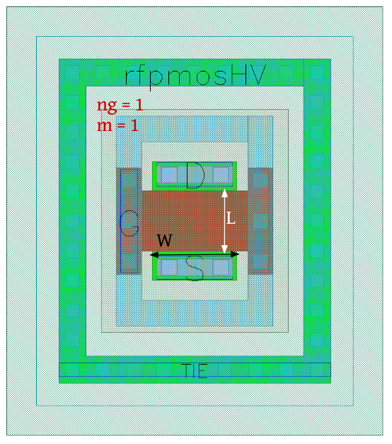
Figure 4.2.4 Layout for RF pMOS-HV transistor