4.4. Diode Devices
4.4.1. dantenna
Device Information
Property |
Value |
|---|---|
Description |
Protection diode for MOS gates. Substrate is anode, metal is cathode. |
Device Recognition |
Activ, Recog.diode |
Model Name |
dantenna |
Layout Cell Name |
sg13g2_pr - dantenna |
Parameters |
w, l, a, p, m |
Netlist Syntax |
D1 GND net1 dantenna w=780.00n l=780.00n a=608.400f p=3.12u m=1 |
Additional Notes |
The anode of the diode should be connected to the ptap1 resistor. |
Parameters Information
Parameter |
Description |
Schematic-View |
LVS-View |
LVS-Comparison |
|---|---|---|---|---|
W |
Active width |
✅ |
❌ |
❌ |
L |
Active length |
✅ |
❌ |
❌ |
A |
Active area |
❌ |
✅ |
✅ |
P |
Active perimeter |
❌ |
✅ |
✅ |
m |
Number of diodes (multiplicity) |
❌ |
✅ |
✅ |
Tip
You have the option to use either W/L or A/P in your netlist.
Layout Information (Refer to Layout Layers)
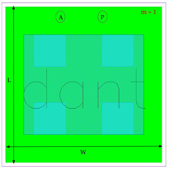
Figure 4.4.1 Layout for dantenna diode device
4.4.2. dpantenna
Device Information
Property |
Value |
|---|---|
Description |
Protection diode for MOS gates. Substrate is cathode, metal is anode. |
Device Recognition |
Activ, Recog.diode, pSD |
Model Name |
dpantenna |
Layout Cell Name |
sg13g2_pr - dpantenna |
Parameters |
w, l, a, p, m |
Netlist Syntax |
D1 GND net1 dpantenna w=780.00n l=780.00n a=608.400f p=3.12u m=1 |
Additional Notes |
The cathode of the diode should be connected to the ntap1 resistor. |
Parameters Information
Parameter |
Description |
Schematic-View |
LVS-View |
LVS-Comparison |
|---|---|---|---|---|
W |
Active width |
✅ |
❌ |
❌ |
L |
Active length |
✅ |
❌ |
❌ |
A |
Active area |
❌ |
✅ |
✅ |
P |
Active perimeter |
❌ |
✅ |
✅ |
m |
Number of diodes (multiplicity) |
❌ |
✅ |
✅ |
Tip
You have the option to use either W/L or A/P in your netlist.
Layout Information (Refer to Layout Layers)
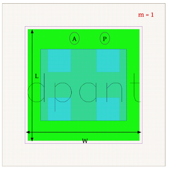
Figure 4.4.2 Layout for dpantenna diode device
4.4.3. schottky_nbl1
Device Information
Property |
Value |
|---|---|
Description |
Schottky Diode. |
Device Recognition |
Activ, metal1, NWell, ThickGateOx, SalBlock, nBuLay, pSD, nSD.blk, PWell.blk, Recog.diode |
Model Name |
schottky_nbl1 |
Layout Cell Name |
sg13g2_pr - schottky_nbl1 |
Parameters |
l, w, m |
Netlist Syntax |
D1 PLUS1 MINUS1 sub! schottky_nbl1 m=1 |
Additional Notes |
Anode is the activ & metal under SalBlock, cathode is the activ & metal inside Nwell. |
Parameters Information
Tip
The schottky_nbl1 device come in predetermined sizes, and the only parameter we keep track of is ‘m’ (multiplicity).
Parameter |
Description |
Schematic-View |
LVS-View |
LVS-Comparison |
|---|---|---|---|---|
W |
ContBar width (Fixed) |
❌ |
❌ |
❌ |
L |
ContBar length (Fixed) |
❌ |
❌ |
❌ |
m |
Number of schottky diodes (multiplicity) |
❌ |
✅ |
✅ |
Layout Information (Refer to Layout Layers)
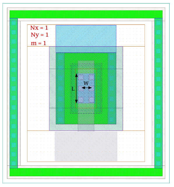
Figure 4.4.3 Layout for schottky_nbl1 diode device