4.7. ESD Devices
Tip
All ESD devices come in predetermined sizes, and the only parameter we keep track of is ‘m’, which is the number of ESD devices (multiplicity).
4.7.1. diodevdd_2k
Device Information
Property |
Value |
|---|---|
Description |
VDD diode. One p+ stripe in n-well. |
Device Recognition |
Activ, pSD, Nwell, Recog.esd |
Model Name |
diodevdd_2kv |
Layout Cell Name |
sg13g2_pr - diodevdd_2kv |
Parameters |
m |
Netlist Syntax |
D1 VDD PAD VSS diodevdd_2kv m=1 |
Additional Notes |
Junction area = 27.78 x 1.26 (x1) um2. |
Parameters Information
Parameter |
Description |
Schematic-View |
LVS-View |
LVS-Comparison |
|---|---|---|---|---|
m |
Number of ESD devices (multiplicity) |
❌ |
✅ |
✅ |
Layout Information (Refer to Layout Layers)
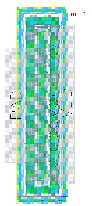
Figure 4.7.1 Layout for diodevdd_2k ESD device
4.7.2. diodevdd_4k
Device Information
Property |
Value |
|---|---|
Description |
VDD diode. Two p+ stripe in n-well. |
Device Recognition |
Activ, pSD, Nwell, Recog.esd |
Model Name |
diodevdd_4kv |
Layout Cell Name |
sg13g2_pr - diodevdd_4kv |
Parameters |
m |
Netlist Syntax |
D1 VDD PAD VSS diodevdd_4kv m=1 |
Additional Notes |
Junction area = 27.78 x 1.26 (x2) um2. |
Parameters Information
Parameter |
Description |
Schematic-View |
LVS-View |
LVS-Comparison |
|---|---|---|---|---|
m |
Number of devices (multiplicity) |
❌ |
✅ |
✅ |
Layout Information (Refer to Layout Layers)
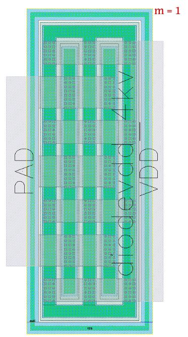
Figure 4.7.2 Layout for diodevdd_4kv ESD device
4.7.3. diodevss_2k
Device Information
Property |
Value |
|---|---|
Description |
VSS diode. One n+ stripe in p-well (Nwell hole). |
Device Recognition |
Activ, pSD, Nwell, Recog.esd |
Model Name |
diodevss_2kv |
Layout Cell Name |
sg13g2_pr - diodevss_2kv |
Parameters |
m |
Netlist Syntax |
D1 VDD PAD VSS diodevss_2kv m=1 |
Additional Notes |
Junction area = 27.78 x 1.26 (x1) um2. |
Parameters Information
Parameter |
Description |
Schematic-View |
LVS-View |
LVS-Comparison |
|---|---|---|---|---|
m |
Number of devices (multiplicity) |
❌ |
✅ |
✅ |
Layout Information (Refer to Layout Layers)
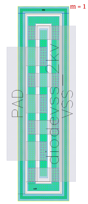
Figure 4.7.3 Layout for diodevss_2k ESD device
4.7.4. diodevss_4k
Device Information
Property |
Value |
|---|---|
Description |
VSS diode. Two n+ stripe in p-well (Nwell hole). |
Device Recognition |
Activ, pSD, Nwell, Recog.esd |
Model Name |
diodevss_4kv |
Layout Cell Name |
sg13g2_pr - diodevss_4kv |
Parameters |
m |
Netlist Syntax |
D1 VDD PAD VSS diodevss_4kv m=1 |
Additional Notes |
Junction area = 27.78 x 1.26 (x2) um2. |
Parameters Information
Parameter |
Description |
Schematic-View |
LVS-View |
LVS-Comparison |
|---|---|---|---|---|
m |
Number of devices (multiplicity) |
❌ |
✅ |
✅ |
Layout Information (Refer to Layout Layers)
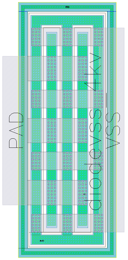
Figure 4.7.4 Layout for diodevss_4kv ESD device
4.7.5. idiodevdd_2k
Device Information
Property |
Value |
|---|---|
Description |
Isolated VDD diode. One p+ stripe in n-well. |
Device Recognition |
Activ, pSD, Nwell, Recog.esd, nBuLay, PWell.blk |
Model Name |
idiodevdd_2kv |
Layout Cell Name |
sg13g2_pr - idiodevdd_2kv |
Parameters |
m |
Netlist Syntax |
D1 VDD PAD VSS idiodevdd_2kv m=1 |
Additional Notes |
Junction area = 27.78 x 1.26 (x1) um2. |
Parameters Information
Parameter |
Description |
Schematic-View |
LVS-View |
LVS-Comparison |
|---|---|---|---|---|
m |
Number of devices (multiplicity) |
❌ |
✅ |
✅ |
Layout Information (Refer to Layout Layers)
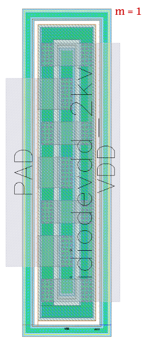
Figure 4.7.5 Layout for idiodevdd_2k ESD device
4.7.6. idiodevdd_4k
Device Information
Property |
Value |
|---|---|
Description |
Isolated VDD diode. Two p+ stripe in n-well. |
Device Recognition |
Activ, pSD, Nwell, Recog.esd |
Model Name |
idiodevdd_4kv |
Layout Cell Name |
sg13g2_pr - idiodevdd_4kv |
Parameters |
m |
Netlist Syntax |
D1 VDD PAD VSS idiodevdd_4kv m=1 |
Additional Notes |
Junction area = 27.78 x 1.26 (x2) um2. |
Parameters Information
Parameter |
Description |
Schematic-View |
LVS-View |
LVS-Comparison |
|---|---|---|---|---|
m |
Number of devices (multiplicity) |
❌ |
✅ |
✅ |
Layout Information (Refer to Layout Layers)
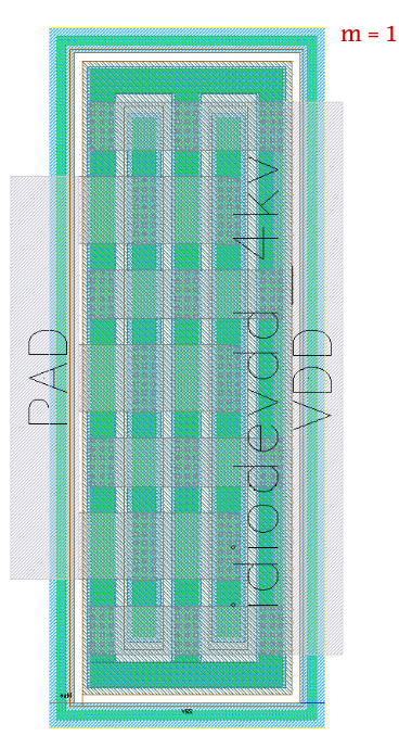
Figure 4.7.6 Layout for idiodevdd_4kv ESD device
4.7.7. idiodevss_2k
Device Information
Property |
Value |
|---|---|
Description |
Isolated VSS diode. One n+ stripe in p-well (Nwell hole). |
Device Recognition |
Activ, pSD, Nwell, Recog.esd |
Model Name |
idiodevss_2kv |
Layout Cell Name |
sg13g2_pr - idiodevss_2kv |
Parameters |
m |
Netlist Syntax |
D1 VDD PAD VSS idiodevss_2kv m=1 |
Additional Notes |
Junction area = 27.78 x 1.26 (x1) um2. |
Parameters Information
Parameter |
Description |
Schematic-View |
LVS-View |
LVS-Comparison |
|---|---|---|---|---|
m |
Number of devices (multiplicity) |
❌ |
✅ |
✅ |
Layout Information (Refer to Layout Layers)
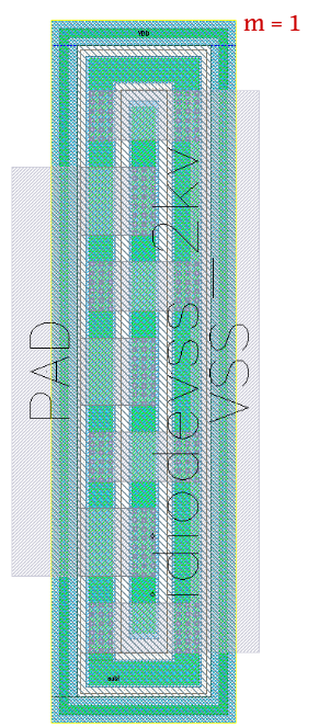
Figure 4.7.5 Layout for idiodevss_2k ESD device
4.7.8. idiodevss_4k
Device Information
Property |
Value |
|---|---|
Description |
Isolated VSS diode. Two n+ stripe in p-well (Nwell hole). |
Device Recognition |
Activ, pSD, Nwell, Recog.esd |
Model Name |
idiodevss_4kv |
Layout Cell Name |
sg13g2_pr - idiodevss_4kv |
Parameters |
m |
Netlist Syntax |
D1 VDD PAD VSS idiodevss_4kv m=1 |
Additional Notes |
Junction area = 27.78 x 1.26 (x2) um2. |
Parameters Information
Parameter |
Description |
Schematic-View |
LVS-View |
LVS-Comparison |
|---|---|---|---|---|
m |
Number of devices (multiplicity) |
❌ |
✅ |
✅ |
Layout Information (Refer to Layout Layers)

Figure 4.7.8 Layout for idiodevss_4kv ESD device
4.7.9. nmoscl_2
Device Information
Property |
Value |
|---|---|
Description |
Isolated NMOS with the silicidation protection mask for the drain region |
Device Recognition |
Activ, GatPoly, pSD, SalBlock, Nwell, nBuLay, Substrate, ThickGateOx, Recog, Recog.esd |
Model Name |
nmoscl_2 |
Layout Cell Name |
sg13g2_pr - nmoscl_2 |
Parameters |
m |
Netlist Syntax |
D1 VDD VSS nmoscl_2 m=1 |
Additional Notes |
This is the grounded gate NMOS device for clamp. |
Corresponding widths are 12 fingers. |
|
Gate length is taken to be always 0.36 um. |
Parameters Information
Parameter |
Description |
Schematic-View |
LVS-View |
LVS-Comparison |
|---|---|---|---|---|
m |
Number of devices (multiplicity) |
❌ |
✅ |
✅ |
Layout Information (Refer to Layout Layers)
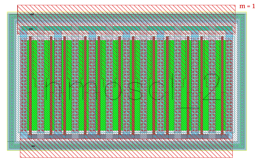
Figure 4.7.9 Layout for nmoscl_2 ESD device
4.7.10. nmoscl_4
Device Information
Property |
Value |
|---|---|
Description |
Isolated NMOS with the silicidation protection mask for the drain region |
Device Recognition |
Activ, GatPoly, pSD, SalBlock, Nwell, nBuLay, Substrate, ThickGateOx, Recog, Recog.esd |
Model Name |
nmoscl_4 |
Layout Cell Name |
sg13g2_pr - nmoscl_4 |
Parameters |
m |
Netlist Syntax |
D1 VDD VSS nmoscl_2 m=1 |
Additional Notes |
This is the grounded gate NMOS device for clamp. |
Corresponding widths are 24 fingers. |
|
Gate length is taken to be always 0.36 um. |
Parameters Information
Parameter |
Description |
Schematic-View |
LVS-View |
LVS-Comparison |
|---|---|---|---|---|
m |
Number of devices (multiplicity) |
❌ |
✅ |
✅ |
Layout Information (Refer to Layout Layers)
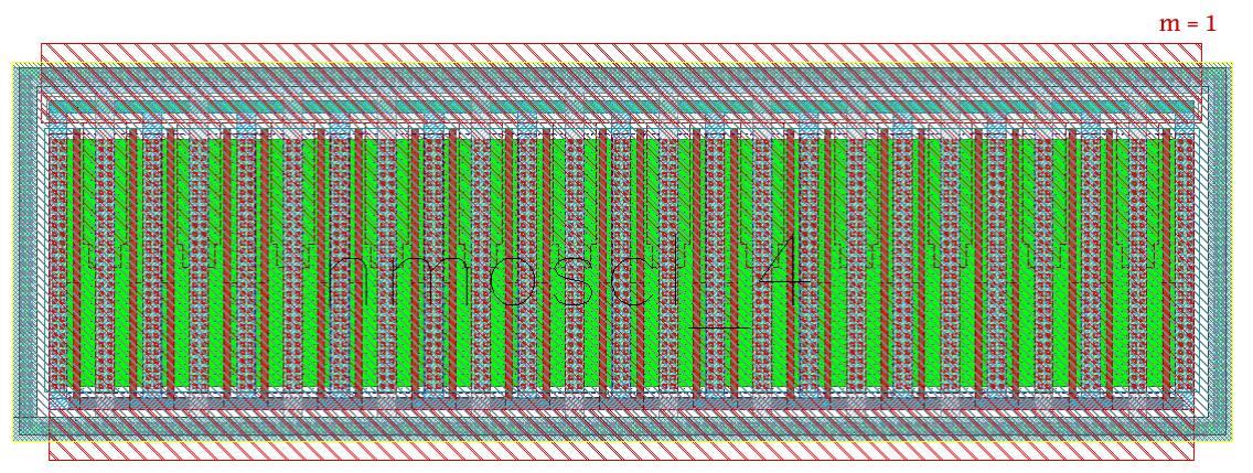
Figure 4.7.10 Layout for nmoscl_4 ESD device
4.7.11. scr1
Note
This device is currently a work in progress.
Device Information
Property |
Value |
|---|---|
Description |
Silicon Control Rectifier (Thyristor) |
Device Recognition |
Activ, GatPoly, pSD, SalBlock, Nwell, nBuLay, Substrate, ThickGateOx, nSD.blk, Recog.esd |
Model Name |
scr1 |
Layout Cell Name |
sg13g2_pr - scr1 |
Parameters |
m |
Parameters Information
Parameter |
Description |
Schematic-View |
LVS-View |
LVS-Comparison |
|---|---|---|---|---|
m |
Number of ESD device (multiplicity) |
❌ |
❌ |
❌ |
Layout Information (Refer to Layout Layers)
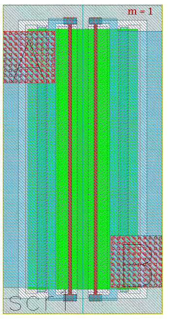
Figure 4.7.11 Layout for scr1 ESD device